CXD2401R Ver la hoja de datos (PDF) - Sony Semiconductor
Número de pieza
componentes Descripción
Fabricante
CXD2401R Datasheet PDF : 21 Pages
| |||
CXD2401R
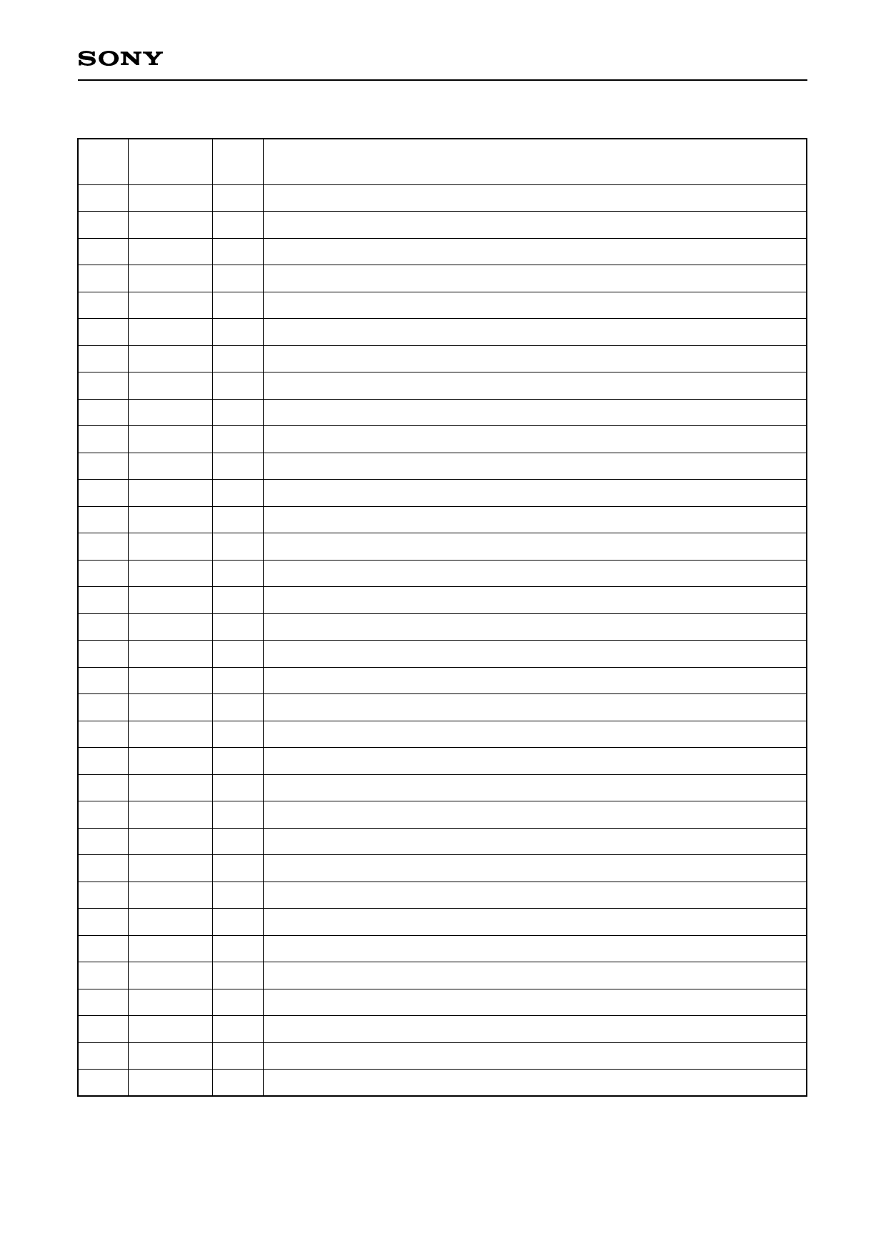
Pin Description
Pin
No.
Symbol
1 OSCI
2 OSCO
3 CK
4 TEST
5 CL
6 VSS1
7 VD
8 HD
9 VDD1
10 CLP4
11 CLP1
12 PBLK
13 ID
14 BFG
15 CLP2
16 VDD2
17 XSHD
18 VSS2
19 XSHP
20 XSP1
21 XSP2
22 XDL1
23 XDL2
24 XV2
25 XV1
26 XSG1
27 XV3
28 XSG2
29 XV4
30 XSUB
31 VSS3
32 H1
33 H2
34 RG
I/O
Description
I Inverter input for oscillation. (NTSC: 1820fH, PAL: 1816fH)
O Inverter output for oscillation. (NTSC: 1820fH, PAL: 1816fH)
I Input for main clock in IC. (NTSC: 1820fH, PAL: 1816fH)
I IC test input. Fixed at GND in normal operation. (With pull-down resistor)
O CK/2 clock output. NTSC: 910fH = 4fsc, PAL: 908fH
— GND
I Vertical sync signal input.
I Horizontal sync signal input.
— 5V power supply.
O Clamping pulse for CCD dummy output.
O Clamping pulse for CCD optical black.
O Cleaning pulse for vertical/horizontal blanking.
O Vertical direction line identification signal.
O Burst flag gate pulse.
O Clamping pulse in horizontal blanking.
— 5V power supply.
O CCD data level sample-and-hold pulse output.
— GND
O CCD precharge level sample-and-hold pulse output.
O Color separation sample-and-hold pulse output.
O Color separation sample-and-hold pulse output.
O Clock output for CCD DL (Delay Line).
O Clock output for CCD DL (Delay Line).
O CCD vertical clock output.
O CCD vertical clock output.
O Clock output for CCD sensor readout.
O CCD vertical clock output.
O Clock output for CCD sensor readout.
O CCD vertical clock output.
O Clock output for CCD electronic shutter.
— GND
O CCD horizontal clock output.
O CCD horizontal clock output.
O CCD reset gate pulse output.
–2–
Share Link: 