TD230 Ver la hoja de datos (PDF) - STMicroelectronics
Número de pieza
componentes Descripción
Fabricante
TD230 Datasheet PDF : 15 Pages
| |||
TD230
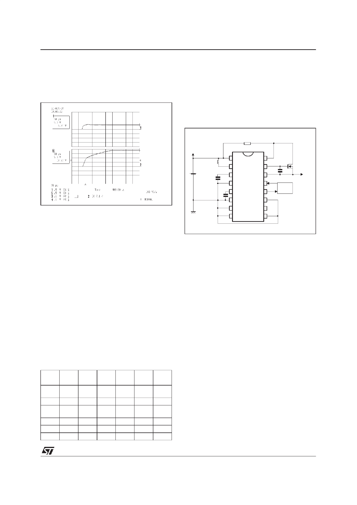
Proper operation of this step-up converter is guar-
anteed at as low as 2.7V with a rise time (0 to 90%
of V(CBOOST)) in the range of 700µs at 2.7V which
Figure 6 : Step Up Converter Rise Time
2.4. Single Supply Breaker Application
The TD230 is perfectly suited to fit in single sup-
plied applications (ex 0-5V), and can drive only one
power MOSFET used as high side power switch.
Figure 7 shows how TD230 can be used as a
single circuit breaker with the same performances.
Figure 7 : Single Electronic Circuit Breaker
Application
is the worst case. At 5V, the rise time of V(Cboost)
is 250µs typ. The CBOOST voltage wave form at
power ON under 5V supply voltage is shown on
figure 6.
Trace 1 represents the power supply voltage (0 to
5V).
Trace 2 represents the CBOOST Voltage at power
ON (0 to 5+13,4 = 18,4V).
Table (a) summerizes the recommended values of
the CBOOST and LBOOST to ensure optimized gate
charge and low ripple voltage with their corre-
sponding maximum current surge (IPK) and nomi-
nal consumption (ICC) of the TD230 for the most
common power supply values. For each power
supply value is also given the recommended value
of a bypass capacitor (CBY) on the power sup-
plies.
Note that both CBOOST and LBOOST are available in
surface mount packages.
Table (a) : Recommended values for Cboost and
Lboost
VCC+ Cboost Lboost
Ipk
Vrip
Icc
Cby
V
nF µH mA mV mA µF
2.7 47 68 60 190 5
>1
100
100
5
100 220 35 120 2.5
1
10 100 470 33 220 2.2
1
220
100
12 220 470 39 150 2.2
1
14 220 680 34 150 2.4
1
18 220 1000 31 200 2.7
1
RS1
Vcc+
LBOOS T
CBOOS T
CTRIP1
GND
P Vcc
1
R EF 1
LBOOS T
2
GC1
CBO OS T
3
S ENS P
4
OS C GND
INHIBIT
5 P M1
S HUTDOWN
6
GND
S ENS N
7
P M2
NVcc
8
GC2
R EF 2
16
NMos
15
CSS 1
to BOARD
14
13
C ONTR OL
12
11
10
9
In this case, the external components consist in :
one boost inductor, one sense resistor, three ca-
pacitors, and one power MOSFET.
2.5. Typical Telecom Line Cards Protection
Application
One of the typical applications where the TD230
can display all its technical advantages is in an
exchange Telecom Cards protection. Sometimes
fifty cards or more are to be supplied with the same
power supply (+/-5V, 1kW), and a decentralized
protection is needed because one card may be
faulty, but should not penalize the others with un-
adapted protection system. The risk of complete
breakdown of the system must be eradicated.
In this application the two above described over
current causes (external line perturbation or inter-
nal component fault) are likely to happen. In the first
case, the current limitation on each card will ensure
undammagingon-board conditions, and in the sec-
ond case, the faulty card will be disjoncted from the
power supply until reset.
Figure 8 shows a typical telecom application with
decentralized protection.
In this application, the positive power supply serves
the logic control and analog signals whereas the
negative power supply is dedicated to the analog.
9/15
Share Link: 