TD230 Ver la hoja de datos (PDF) - STMicroelectronics
Número de pieza
componentes Descripción
Fabricante
TD230 Datasheet PDF : 15 Pages
| |||
TD230
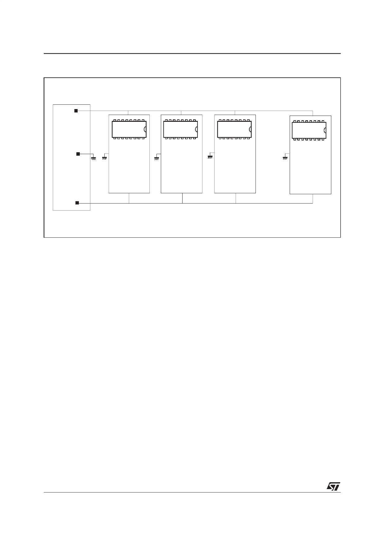
Figure 8 : Decentralized Protection
Vcc+
P owe r S upply
GND
Vcc-
TD2 30
TD2 30
BOARD1
BOARD2
TD2 30
BOARD3
TD230
BOARDN
Therefore, when a fault appears onthe positive rail,
the definitive shutdown of the positive NMOS will
lead to the shutdown of the negative NMOS, but
when a fault appears on the negative rail, the
definitive shutdown of the negativeNMOS will have
no effect on the positive NMOS.
Several possibilities are offered to reset the whole
system when it has been led to definitive
shutdown :
• the card can be unplugged and plugged back
(live insertion)
• the INHIBIT pin can be set to active state dur-
ing a short time (100µs typ or more) in the
case of remote control facilities
3. PERFORMANCES AND EVALUATION
All the curves shown in this application note have
been realized with the TD230 Evaluation Board.
The external conditions and components were as
listed hereafter :
• Vcc+ = 5V
• Vcc- = -5V
• Suppliable output short circuit current = 5A
• IC = TD230
• MOSFET 1 = BUZ71
• MOSFET 2 = BUZ71
• LBOOST = 220µH
• CBOOST = 100nF
• CTRIP1 = 10µF
• CTRIP2 = 10µF
• RS1 = 68mΩ
• RS2 = 68mΩ
• CSS1 = 1nF
• CSS2 = 1nF
• Positive Bypass = 4.7µF (plastic)
• Negative Bypass = 4.7µF (plastic)
The evaluation board is available and allows to test
the performances of the TD230. The layout and
schematic of this evaluation board are given on
figures 9A-9B-9C.
4. CAUTIONS
For proper use of the TD230 as a reliable protection
device, a few precautions must be taken :
1. Proper bypass capacitors must be connected as
close as possible to the power pins of the TD230
(PVcc, NVcc, GND). Some recommended values
are given in table (a).
2. The OSCGND pin must be tied to the GND pin
externally (printed board) to ensure proper step-up
converter reference. If not, the step-up converter
will not start.
3. TheINHIBIT pin is a CMOS/TTL compatible input
which should therefore not be left unconnected.
The absolute maximum rating of this input is 7V. It
should be tied to the TTL compatible output of an
10/15
Share Link: 