MC145406 Ver la hoja de datos (PDF) - Philips Electronics
Número de pieza
componentes Descripción
Fabricante
MC145406 Datasheet PDF : 5 Pages
| |||
Philips Semiconductors Linear Products
EIA-232-D/V.28 driver/receiver
Product specification
MC145406
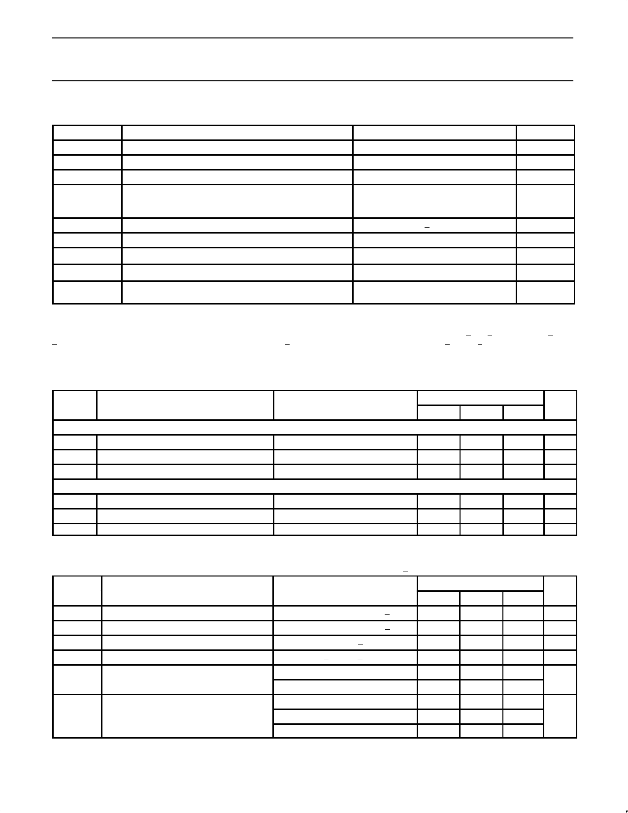
ABSOLUTE MAXIMUM RATINGS
SYMBOL
PARAMETER
VCC
Supply voltage
VDD
Supply voltage
VSS
Supply voltage
Input voltage range
VIR
RX1-3 inputs
DI1-3 inputs
DC current per pin
PD
Power dissipation (package)
TA
Operating temperature range
TSTG
θJA
Storage temperature range
Thermal impedance N package
D package
RATING
-0.5 to +6.0
-0.5 to +13.5
+0.5 to -13.5
(VSS - 15) to (VDD + 15)
-0.5 to (VCC + 0.5)
+100
1.0
0 to +70
-65 to +150
80
105
UNITS
V
V
V
V
mA
W
°C
°C
°C/W
NOTE: This device contains protection circuitry to protect the inputs against damage due to high static voltages or electric fields; however, it is
advised that normal precautions be taken to avoid application of any voltage higher than maximum rated voltages to this high impedance circuit.
For proper operation, it is recommended that the voltages at the DI and DO pins be constrained to the range GND < VDI < VDD and GND < VDO
< VCC. Also, the voltage at the RX pin should be constrained to +25V, and TX should be constrained to VSS < VTX1-3 < VDD. Unused inputs
must always be tied to an appropriate logic voltage level (e.g., GND or VCC for DI, and VSS or VDD for RX).
DC ELECTRICAL CHARACTERISTICS
Typical values are at TA = 0 to 70°C; GND = 0V, unless otherwise specified.
SYMBOL
PARAMETER
TEST CONDITIONS
DC supply voltage
VDD
VSS
VCC
Quiescent supply current (outputs unloaded, inputs low)
IDD
ISS
ICC
VDD = +12V
VSS = -12V
VCC = +5V
LIMITS
UNITS
MIN
TYP
MAX
4.5
5 to 12
13.2
V
-4.5 -5 to -12 -13.2
V
4.5
5.0
5.5
V
20
400
µA
280
600
µA
260
450
µA
RECEIVER ELECTRICAL CHARACTERISTICS
Typical values are at TA = 0 to 70°C; GND = 0V; VDD = +5 to +12V; VSS = -5 to -12V; VCC = +5V +5%, unless otherwise specified.
SYMBOL
PARAMETER
TEST CONDITIONS
LIMITS
MIN
TYP
MAX
VON
VOFF
VON-VOFF
RIN
VOH
Input turn-on threshold
Input turn-off threshold
Input threshold hysteresis
Input resistance
High level output voltage
VRX1-3 = -3V to (VSS-15V)1
RX1-3
RX1-3
RX1-3
RX1-3
DO1-3
VOL
Low level output voltage
DO1-3
VRX1-3 = +3V to (VDD+15V)1
VDO1-3 = VOL, VCC = 5.0V +5%
VDO1-3 = VOH, VCC = 5.0V +5%
VCC = 5.0V +5%
(VSS-15V) < VRX1-3 < (VDD+15V)
IOH = -20µA, VCC = +5.0V
IOH = -1mA, VCC = +5.0V
IOL = +20µA, VCC = +5.0V
IOL = +2mA, VCC = +5.0V
IOL = +4mA, VCC = +5.0V
1.35
0.75
0.6
3.0
4.9
3.8
1.80
1.00
0.8
5.0
5.0
4.4
0.005
0.15
0.3
2.35
1.25
7.0
0.1
0.5
0.7
NOTE:
1. This is the range of input voltages as specified by EIA-232-D to cause a receiver to be in the high or low logic state.
UNITS
V
V
V
kΩ
V
V
August 31, 1994
469
Share Link: 