LM219 Ver la hoja de datos (PDF) - Philips Electronics
Número de pieza
componentes Descripción
Fabricante
LM219 Datasheet PDF : 5 Pages
| |||
Philips Semiconductors Linear Products
Dual voltage comparator
Product specification
LM219/319
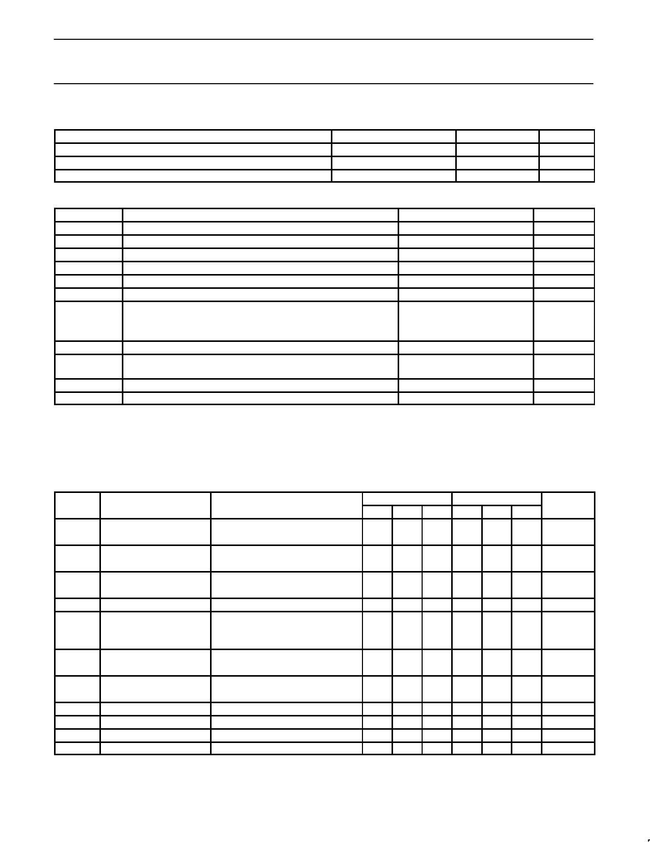
ORDERING INFORMATION
DESCRIPTION
14-Pin Plastic Small Outline (SO) Package
14-Pin Plastic Small Outline (SO) Package
14-Pin Plastic Dual In-Line Package (DIP)
TEMPERATURE RANGE
-25 to +85°C
0 to +70°C
0 to +70°C
ORDER CODE
LM219D
LM319D
LM319N
DWG #
0175D
0175D
0405B
ABSOLUTE MAXIMUM RATINGS
SYMBOL
PARAMETER
VS
Total supply voltage
Output to negative supply voltage
Ground to negative supply voltage
Ground to positive supply voltage
Differential input voltage
VIN
Input voltage1
Maximum power dissipation, TA=25°C (still-air)2
N package
D package
Output short-circuit duration
Operating temperature range
LM219
TA
LM319
TSTG
Storage temperature range
TSOLD
Lead soldering temperature (10sec max)
NOTES:
1. For supply voltages less than ±15V, the absolute maximum rating is equal to the supply voltage.
2. Derate above 25°C, at the following rates:
N package at 11.4mW/°C
D package at 8.3mW/°C
RATING
36
36
25
18
±5
±15
1420
1040
10
-25 to +85
0 to +70
-65 to +150
300
UNIT
V
V
V
V
V
V
mW
mW
s
°C
°C
°C
DC ELECTRICAL CHARACTERISTICS
VS=±15V, -25°C ≤ TA ≤ 85°C for LM219, 0°C ≤ TA ≤ 70°C for LM319, unless otherwise specified.
SYMBOL PARAMETER
TEST CONDITIONS
LM219
LM319
Min Typ Max Min Typ Max
UNIT
VOS
Input offset voltage1, 2
RS≤5kΩ, TA=25°C
Over temp.
0.7 4.0
7
2.0 8.0
mV
10
IOS
Input offset current1, 2
TA=25°C
Over temp.
30 75
100
80 200
nA
300
IB
Input bias current1
TA=25°C
Over temp.
150 500
1000
250 1000
nA
1200
nA
AV
Voltage gain
TA=25°C
8
40
8
40
V/mV
VOL
Saturation voltage
VIN≤-10mV, IOUT=25mA, TA=25°C,
V+≥4.5V, V-=0
0.75 1.5
0.75 1.5
V
VIN≤-10mV, IOUT=3.2mA
0.3 0.6
0.3 0.4
IOH
Output leakage current
V-=0V, VIN≥10mV
VOUT=35V, TA=25°C
0.2 10
0.2 10
µA
VIN
Input voltage range
VS=±15V
V+=5V, V-=0V
±13
±13
V
1
3
1
3
VID
Differential input voltage
±5
±5
V
I+
Positive supply current
V+=5V, V-=0V, TA=25°C
4.3
4.3
mA
I+
Positive supply current
VS=±15V, TA=25°C
8.0 12.5
8.0 12.5
mA
I-
Negative supply current
VS=±15V, TA=25°C
3.0 5.0
3.0 5.0
mA
NOTES:
1. VOS, IOS and IB specifications apply for a supply voltage range of VS=±15V down to a single 5V supply.
2. The offset voltages and offset currents given are the maximum values required to drive the output to within 1V of either supply with a 1mA
load. Thus these parameters define an error band and take into account the worst case effects of voltage gain and input impedance.
August 31, 1994
278
Share Link: 