VSC7130 Ver la hoja de datos (PDF) - Vitesse Semiconductor
Número de pieza
componentes Descripción
Fabricante
VSC7130 Datasheet PDF : 22 Pages
| |||
VITESSE
SEMICONDUCTOR CORPORATION
Dual Repeater/Retimer
for Fibre Channel and Gigabit Ethernet
Data Sheet
VSC7130
Input and Output Buffers, Analog Signal Detection, Cable Equalization
The RX0+/-, RX1+/- and SI+/- differential inputs are high performance input buffers which amplify the
incoming signal. Furthermore, a cable equalization circuit is included in the input buffer which accentuates
high frequency signals in order to compensate for the high frequency loss found in copper cables and traces.
This cable equalization circuit enhances the ability of the VSC7130 to reliably receive serial inputs which have
been degraded with jitter. The RX1+/- input buffer also includes an analog signal detection circuit which has
adjustable thresholds set by the external RXBIAS pin (see Figure 9). The output of this signal is processed fur-
ther in the Signal Detection circuitry described elsewhere, as well as selectable threshold levels which are
selected with the RXBIAS input.
If the Two-Wire Interface is not used, R1/0 directly controls the RX0 and RX1 input buffers and Cable
Equalization is enabled in SI, RX0 and RX1. If the Two-Wire Interface is used, microcontroller control allows
enabling or disabling of the cable equalization circuit.
Please refer to the VSC7130 User’s Manual for a more complete description of the input and output buffer
controls and cable equalization controls.
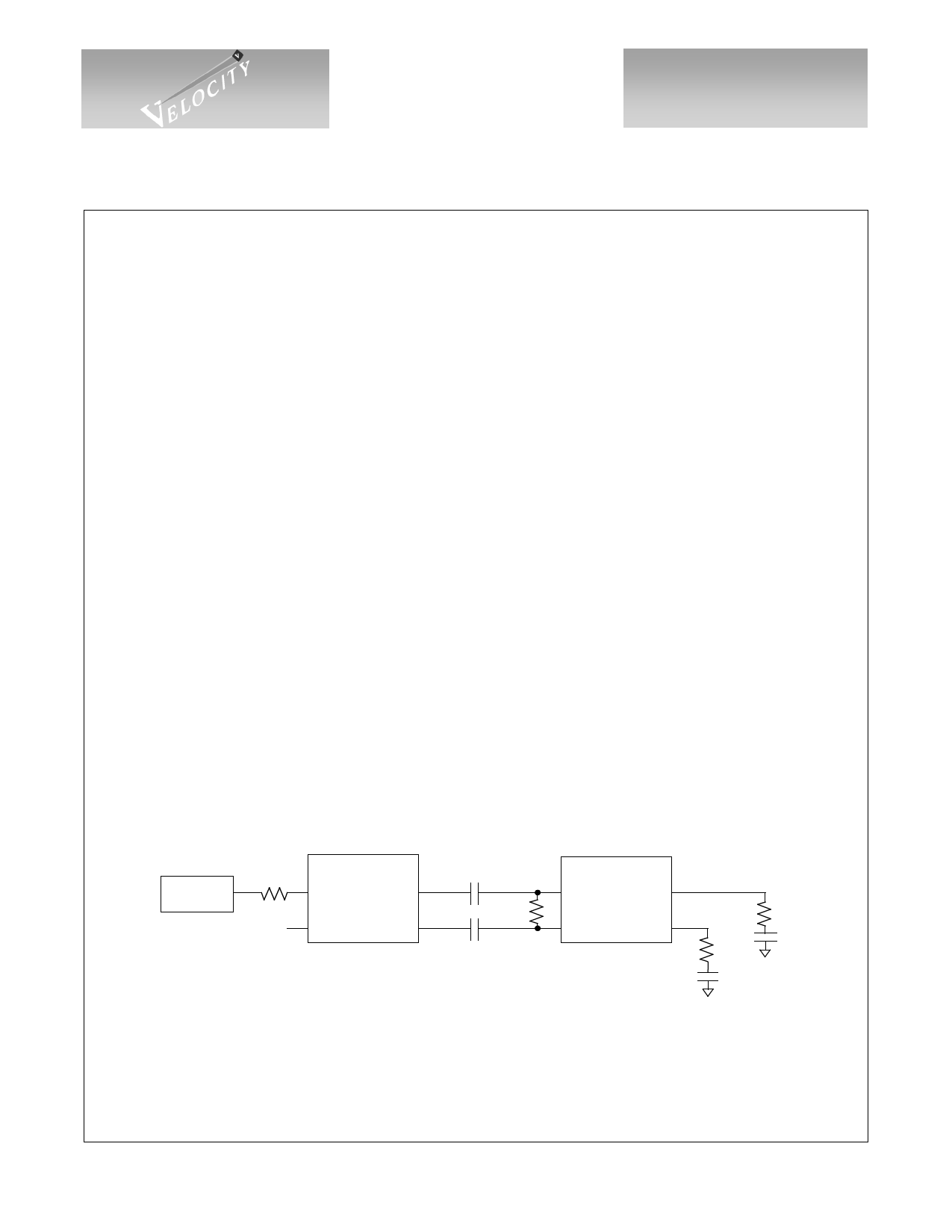
High-Speed I/O Termination Schemes
The high-speed I/O lines for the VSC7130 require the standard Vitesse 1Gb/s CMOS device termination
schemes. Please refer to the Termination for 1Gb/s CMOS Devices Application Note (AN-54) for VSC7130 RX
and TX termination schemes. When using the REFI+/- and REFO+/- pins on the VSC7130 in daisy-chained
clock applications, specific termination must be implemented. If the REFO+/- pins of one VSC7130 are to be
routed to the REFI+/- pins of a second VSC7130, 50Ω single-ended (100Ω differential) traces should be used.
AC coupling caps should be placed between the two VSC7130s. Additionally, a 100Ω 1% termination resistor
should be place between the REFI+ and REFI- lines of the second VSC7130. This termination resistor should
be located as close to the REFI+/- pins as possible. Figure 6 shows the recommended termination and compo-
nents when using the VSC7130’s REFI and REFO.
Figure 6: REFI and REFO Recommended Termination
53.125 or 106.25MHz
Oscillator
22Ω
(TTL)
X
VSC7130 #1
REFI+ REFO+
REFI- REFO-
0.01µF
100Ω
1%
0.01µF
VSC7130 #2
REFI+ REFO+
REFI- REFO-
50Ω
1%
50Ω
0.01µF
1%
0.01µF
Page 6
© VITESSE SEMICONDUCTOR CORPORATION • 741 Calle Plano • Camarillo, CA 93012
Tel: (800) VITESSE • FAX: (805) 987-5896 • Email: prodinfo@vitesse.com
Internet: www.vitesse.com
G52297-0, Rev 4.0
04/02/01
Share Link: 