MC330077D Ver la hoja de datos (PDF) - Motorola => Freescale
Número de pieza
componentes Descripción
Fabricante
MC330077D Datasheet PDF : 12 Pages
| |||
MC33077
occur, the amplifier’s phase will degrade severely causing the
amplifier to become unstable. Effective source resistances,
acting in conjunction with the input capacitance of the
amplifier, should be kept to a minimum to avoid creating such
a pole at the input (see Figure 31). There is minimal effect on
stability where the created input pole is much greater than the
closed loop corner frequency. Where amplifier stability is
affected as a result of a negative feedback resistor in
conjunction with the amplifier’s input capacitance, creating a
pole near the closed loop corner frequency, lead capacitor
compensation techniques (lead capacitor in parallel with the
feedback resistor) can be employed to improve stability. The
feedback resistor and lead capacitor RC time constant
should be larger than that of the uncompensated input pole
frequency. Having a high resistance connected to the
noninverting input of the amplifier can create a like instability
problem. Compensation for this condition can be
accomplished by adding a lead capacitor in parallel with the
noninverting input resistor of such a value as to make the RC
time constant larger than the RC time constant of the
uncompensated input resistor acting in conjunction with the
amplifiers input capacitance.
For optimum frequency performance and stability, careful
component placement and printed circuit board layout should
be exercised. For example, long unshielded input or output
leads may result in unwanted input output coupling. In order
to reduce the input capacitance, the body of resistors
connected to the input pins should be physically close to the
input pins. This not only minimizes the input pole creation for
optimum frequency response, but also minimizes extraneous
signal “pickup” at this node. Power supplies should be
decoupled with adequate capacitance as close as possible to
the device supply pin.
In addition to amplifier stability considerations, input
source resistance values should be low to take full advantage
of the low noise characteristics of the amplifier. Thermal
noise (Johnson Noise) of a resistor is generated by
thermally–charged carriers randomly moving within the
resistor creating a voltage. The rms thermal noise voltage in
a resistor can be calculated from:
Enr = / 4k TR × BW
where:
k = Boltzmann’s Constant (1.38 × 10⁻²³ joules/k)
T = Kelvin temperature
R = Resistance in ohms
BW = Upper and lower frequency limit in Hertz.
By way of reference, a 1.0 kΩ resistor at 25°C will produce
a 4.0 nV/√Hz of rms noise voltage. If this resistor is
connected to the input of the amplifier, the noise voltage will
be gained–up in accordance to the amplifier’s gain
configuration. For this reason, the selection of input source
resistance for low noise circuit applications warrants serious
consideration. The total noise of the amplifier, as referred to
its inputs, is typically only 4.4 nV/√Hz at 1.0 kHz.
The output of any one amplifier is current limited and thus
protected from a direct short to ground, However, under such
conditions, it is important not to allow the amplifier to exceed
the maximum junction temperature rating. Typically for ±15 V
supplies, any one output can be shorted continuously to
ground without exceeding the temperature rating.
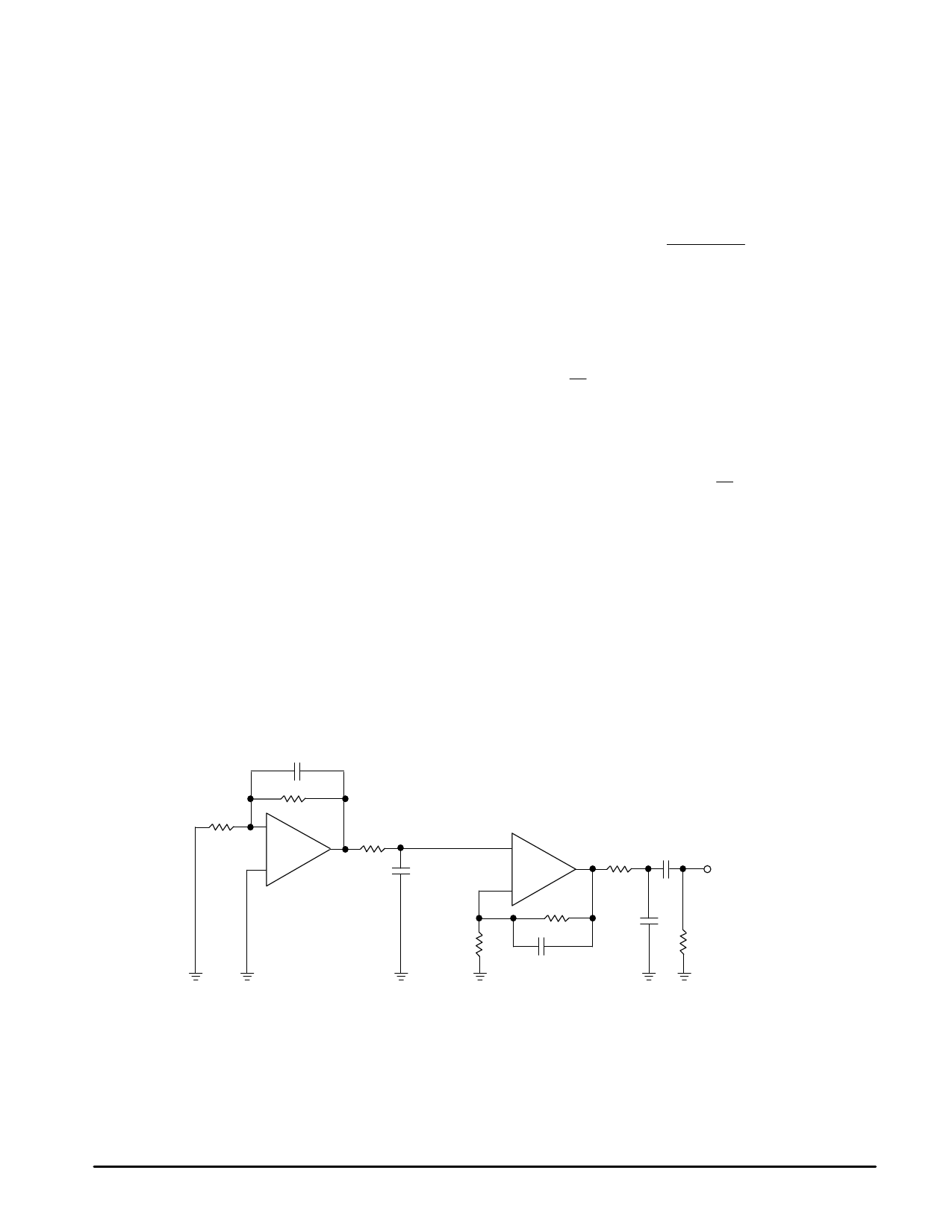
0.1 µF
Figure 36. Voltage Noise Test Circuit
(0.1 Hz to 10 Hzp–p)
10 Ω
100 kΩ
–
2.0 kΩ
D.U.T.
+
4.7 µF
Voltage Gain = 50,000
24.3 kΩ
+
1/2
MC33077
–
100 kΩ
0.1 µF
4.3 kΩ
2.2 µF
22 µF
Scope
×1
Rin = 1.0 MΩ
110 kΩ
Note: All capacitors are non–polarized.
MOTOROLA ANALOG IC DEVICE DATA
11
Share Link: 