4N25-X016 Ver la hoja de datos (PDF) - Vishay Semiconductors
Número de pieza
componentes Descripción
Fabricante
4N25-X016 Datasheet PDF : 7 Pages
| |||
www.vishay.com
4N25-X, 4N26-X, 4N27-X, 4N28-X
Vishay Semiconductors
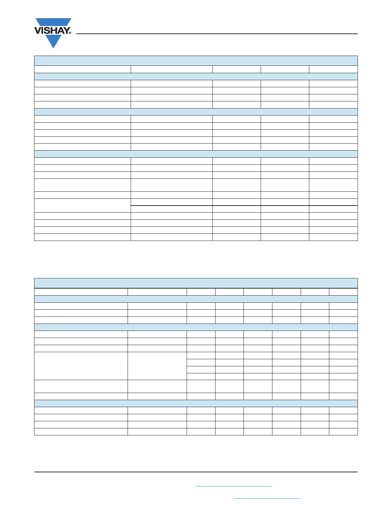
ABSOLUTE MAXIMUM RATINGS (Tamb = 25 °C, unless otherwise specified)
PARAMETER
TEST CONDITION
SYMBOL
VALUE
UNIT
INPUT
Reverse voltage
Forward current
Surge current
Power dissipation
OUTPUT
t ≤ 10 μs
VR
6
V
IF
60
mA
IFSM
2.5
A
Pdiss
70
mW
Collector emitter breakdown voltage
VCEO
70
V
Emitter base breakdown voltage
VEBO
7
V
Collector current
IC
50
mA
Collector peak current
tp/T = 0.5, tp ≤ 10 ms
ICM
100
mA
Output power dissipation
Pdiss
150
mW
COUPLER
Isolation test voltage
Creepage distance
VISO
5000
≥7
VRMS
mm
Clearance distance
≥7
mm
Isolation thickness between emitter and
detector
≥ 0.4
mm
Comparative tracking index
DIN IEC 112/VDE0303, part 1
≥ 175
Isolation resistance
Storage temperature
Operating temperature
Junction temperature
Soldering temperature (1)
VIO = 500 V, Tamb = 25 °C
RIO
≥ 1012
Ω
VIO = 500 V, Tamb = 100 °C
RIO
≥ 1011
Ω
Tstg
- 55 to + 150
°C
Tamb
- 55 to + 100
°C
Tj
100
°C
2 mm from case, ≤ 10 s
Tsld
260
°C
Notes
• Stresses in excess of the absolute maximum ratings can cause permanent damage to the device. Functional operation of the device is not
implied at these or any other conditions in excess of those given in the operational sections of this document. Exposure to absolute
maximum ratings for extended periods of the time can adversely affect reliability.
(1) Refer to reflow profile for soldering conditions for surface mounted devices (SMD). Refer to wave profile for soldering conditions for through
hole devices (DIP).
ELECTRICAL CHARACTERISTICS (Tamb = 25 °C, unless otherwise specified)
PARAMETER
TEST CONDITION
PART SYMBOL MIN.
TYP.
MAX.
UNIT
INPUT
Forward voltage (1)
Reverse current (1)
Capacitance
OUTPUT
IF = 50 mA
VR = 3.0 V
VR = 0 V
VF
1.36
1.5
V
IR
0.1
100
μA
CO
25
pF
Collector base breakdown voltage (1)
IC = 100 μA
BVCBO
70
V
Collector emitter breakdown voltage(1)
IC = 1.0 mA
BVCEO
30
V
Emitter collector breakdown voltage (1)
IE = 100 μA
BVECO
7
V
4N25
5
50
nA
ICEO(dark) (1)
VCE = 10 V, (base open)
4N26
4N27
5
50
nA
5
50
nA
4N28
10
100
nA
ICBO(dark) (1)
VCB = 10 V,
(emitter open)
2.0
20
nA
Collector emitter capacitance
COUPLER
VCE = 0
CCE
6.0
pF
Isolation test voltage (1)
Saturation voltage, collector emitter
Resistance, input output (1)
Capacitance, input output
Peak, 60 Hz
ICE = 2.0 mA, IF = 50 mA
VIO = 500 V
f = 1 MHz
VIO
5000
V
VCE(sat)
0.5
V
RIO
100
GΩ
CIO
0.5
pF
Notes
• Minimum and maximum values are testing requirements. Typical values are characteristics of the device and are the result of engineering
evaluation. Typical values are for information only and are not part of the testing requirements.
(1) JEDEC registered values are 2500 V, 1500 V, 1500 V and 500 V for the 4N25, 4N26, 4N27, and 4N28 respectively.
Rev. 1.2, 16-Jan-12
2
Document Number: 81864
For technical questions, contact: optocoupleranswers@vishay.com
THIS DOCUMENT IS SUBJECT TO CHANGE WITHOUT NOTICE. THE PRODUCTS DESCRIBED HEREIN AND THIS DOCUMENT
ARE SUBJECT TO SPECIFIC DISCLAIMERS, SET FORTH AT www.vishay.com/doc?91000
Share Link: 