OP275 Ver la hoja de datos (PDF) - Analog Devices
Número de pieza
componentes Descripción
Fabricante
OP275 Datasheet PDF : 12 Pages
| |||
OP275
APPLICATIONS
Circuit Protection
OP275 has been designed with inherent short-circuit protection
to ground. An internal 30 resistor, in series with the output,
limits the output current at room temperature to ISC+ = 40 mA
and ISC– = –90 mA, typically, with ±15 V supplies.
However, shorts to either supply may destroy the device when
excessive voltages or currents are applied. If it is possible for a
user to short an output to a supply for safe operation, the output
current of the OP275 should be design-limited to ±30 mA, as
shown in Figure 1.
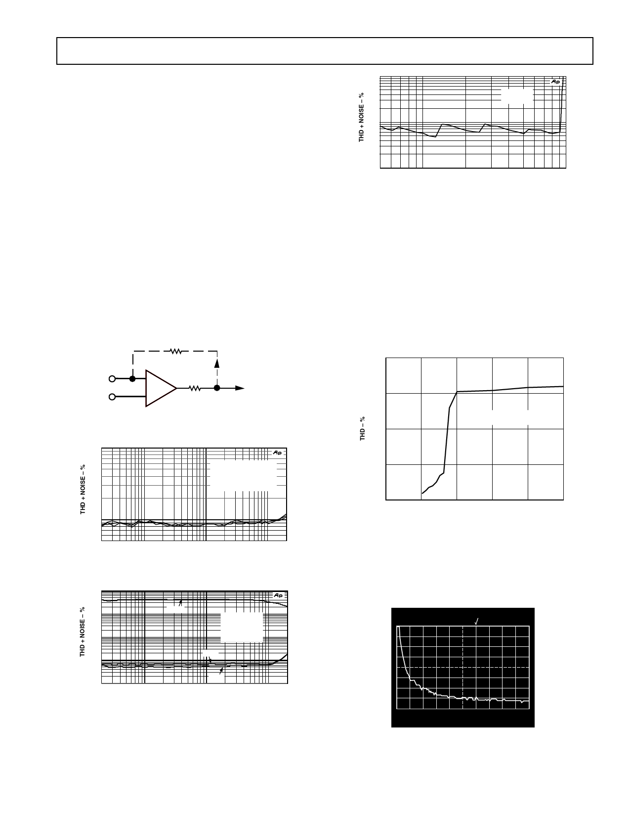
Total Harmonic Distortion
Total Harmonic Distortion + Noise (THD + N) of the OP275 is
well below 0.001% with any load down to 600 . However, this is
dependent upon the peak output swing. In Figure 2, the THD +
Noise with 3 V rms output is below 0.001%. In Figure 3, THD +
Noise is below 0.001% for the 10 k and 2 k loads but increases
to above 0.1% for the 600 load condition. This is a result of the
output swing capability of the OP275. Notice the results in Figure 4,
showing THD versus VIN (V rms). This figure shows that the THD
+ Noise remains very low until the output reaches 9.5 V rms. This
performance is similar to competitive products.
RFB
FEEDBACK
–
RX
332
A1
VOUT
+
A1 = 1/2 OP275
Figure 1. Recommended Output Short-Circuit Protection
0.010
RL = 600, 2k, 10k
VS = 15V
VIN = 3V rms
AV = +1
0.001
0.0005
20
100
1k
FREQUENCY – Hz
10k 20k
Figure 2. THD + Noise vs. Frequency vs. RLOAD
1
0.1
0.010
0.001
600
AV = +1
VS = 18V
VIN = 10V rms
80kHz FILTER
2k
0.0001
20
10k
100
1k
FREQUENCY – Hz
10k 20k
Figure 3. THD + Noise vs. RLOAD; VIN =10 V rms
0.010
0.001
VS = 18V
RL = 600
0.0001
0.5
1
10
OUTPUT SWING – V rms
Figure 4. Headroom, THD + Noise vs. Output
Amplitude (V rms); RLOAD = 600 , VSUP = ±18 V
The output of the OP275 is designed to maintain low harmonic
distortion while driving 600 loads. However, driving 600
loads with very high output swings results in higher distortion if
clipping occurs. A common example of this is in attempting to
drive 10 V rms into any load with ±15 V supplies. Clipping will
occur and distortion will be very high. To attain low harmonic
distortion with large output swings, supply voltages may be
increased. Figure 5 shows the performance of the OP275 driving
600 loads with supply voltages varying from ±18 V to ±20 V.
Notice that with ±18 V supplies the distortion is fairly high, while
with ±20 V supplies it is a very low 0.0007%.
0.0001
0.001
0.01
RL = 600
VOUT = 10V rms @ 1kHz
0.1
0
17
18
19
20
21
22
SUPPLY VOLTAGE – V
Figure 5. THD + Noise vs. Supply Voltage
Noise
The voltage noise density of the OP275 is below 7 nV/Hz from
30 Hz. This enables low noise designs to have good performance
throughout the full audio range. Figure 6 shows a typical OP275
with a 1/f corner at 2.24 Hz.
CH A: 80.0V FS
10.0V/DIV
MKR: 45.6V/ Hz
0Hz
MKR: 2.24Hz
10Hz
BW: 0.145Hz
Figure 6. 1/f Noise Corner, VS = ±15 V, AV = 1000
REV. C
–7–
Share Link: 