1EDI30J12CP Ver la hoja de datos (PDF) - Unspecified
Número de pieza
componentes Descripción
Fabricante
1EDI30J12CP Datasheet PDF : 28 Pages
| |||
EiceDRIVER™ Enhanced
1EDI30J12CP
Characteristics
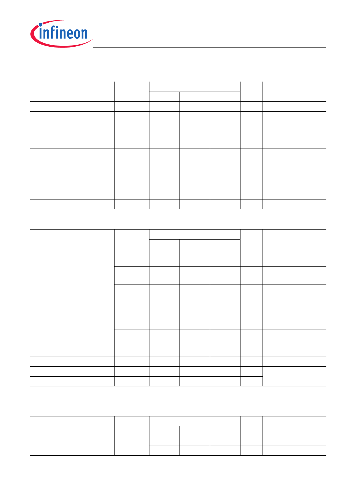
Table 6 Logic Input
Parameter
IN, EN low input voltage
IN, EN high input voltage
IN, EN input current
BSEN low input voltage
BSEN high input voltage
BSEN output current
BSEN output current
Symbol
VINL
VINH
ΙIN
VBSENL
VBSENH
ΙBSEN
ΙBSENPD
Min.
2.0
VVREG +
3.0
-70
Values
Typ.
Max.
1.0
30
400
VVREG +
2.0
-3.5
-2
-38
-15
Unit
V
V
µA
V
V
mA
µA
Note / Test Condition
VIN=VVCC1
VBSEN > VVREG + 5.7V,
VIN = high,
VVREGon < VVREG <
VVREGonBS
VIN= low
Table 7 JFET Driver (Reference is VCC2)
Parameter
Symbol
Min.
High Level Output Voltage
VJFDrvH
-2.0
Values
Typ.
-1.75
Max.
Unit Note / Test Condition
V
IJFDrv=200mA;
-4.0
-3.5
V
IJFDrv=2A;
—
-4.1
V
High Level Output Peak
IJFDrvH
3.0
4.0
A
Current
Output Voltage at low state
VJFDrvL
VVREG + VVREG + V
0.17
0.35
VVREG + VVREG + V
1.9
4.0
—
3.0
V
Low Level Output Peak Current IJFDrvL
-3.0
-4.0
A
Rise Time JFDrv
tJFDrvR
—
23
30
ns
Fall Time JFDrv
tJFDrvF
—
22
35
ns
1) The parameter is not subject to production test - verified by design/characterisation
IJFDrv=3A1)
1)
IJFDrv=-200mA;
IJFDrv=-2A;
IJFDrv=-3A1)
1)
CLOADJ= 4.7 nF,
VL=20% to VH 80%
Table 8 MOSFET Driver (Reference is VCC2)
Parameter
Symbol
Min.
High Level Output Voltage
VMDrvH
-1.75
-4.0
Values
Typ.
-1.35
-3.15
Max.
Unit Note / Test Condition
V
IMDrv=150mA
V
IMDrv=1.5A
Preliminary Datasheet
17
Rev. 1.3, 2014-11-12
Share Link: 