1EDI30J12CP Ver la hoja de datos (PDF) - Unspecified
Número de pieza
componentes Descripción
Fabricante
1EDI30J12CP Datasheet PDF : 28 Pages
| |||
EiceDRIVER™ Enhanced
1EDI30J12CP
Functional Description
datasheet values of typical 80ns. A timing diagram showing the various signals in this startup mode is depicted in
Figure 7. Figure 8 shows a diagram detailing the reason for the prolonged popagation delay.
The longer propagation delay can be indicated to the input side by using an optocoupler. The optocoupler diode
is inserted between BSEN and VCC2. During the start up phase in bootstrap mode BSEN is applying an output
current of at least 2 mA while IN is high.
During the bootstrap start up phase the power dissipation in the driver is increased. Therefore, the controller has
to make sure that the driver does not remain in bootstrap start up mode for longer periods of time in order not to
overheat the driver.
During the boostrap start-up phase, the propagation delay is larger and the effective JFET conduction time shorter
compared to standard operating mode. This means, the controller has to take care to compensate for the longer
propagation delays and shorter on-times, e.g. in a half-bridge configuration, the dead-times have to be increased.
After the start-up phase is finished, the controller has to reduce the dead-times to normal operating values, not to
risk body-diode conduction over long periods of time, which can lead to higher power dissipation of the JFETs.
800V
+5V
CVCC1
GND
LS_IN
VCC1 JFDrv
VCC2
GND1 MDrv
EN
VReg
IN
CLJFG
VEE2
BSEN
1EDI30J12Cx
CVReg CVEE2
+5V
CVCC1
GND
LS_IN
VCC1 JFDrv
VCC2
GND1 MDrv
EN
VReg
IN
CLJFG
VEE2
BSEN
1EDI30J12Cx
CVReg CVEE2
C
-25V_H
+5V
CVCC1
GND
LS_IN
VCC1 JFDrv
VCC2
GND1 MDrv
EN
VReg
IN
CLJFG
VEE2
BSEN
1EDI30J12Cx
CVReg
CVEE2
+5V
CVCC1
GND
LS_IN
VCC1 JFDrv
VCC2
GND1 MDrv
EN
VREG
IN
CLJFG
VEE2
BSEN
1EDI30J12Cx
CVReg
CVEE2
C
-25V
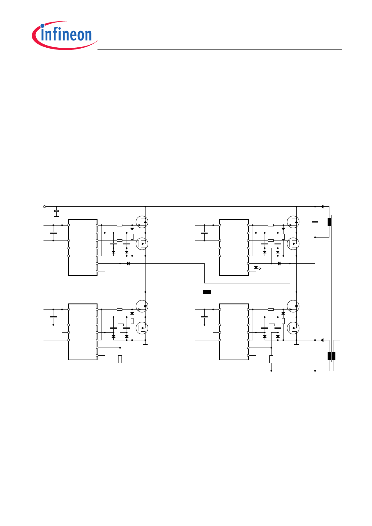
Figure 6 Application drawing for high side bootstrap supply (FB)
Preliminary Datasheet
11
Rev. 1.3, 2014-11-12
Share Link: 