IDT72V275 Ver la hoja de datos (PDF) - Unspecified
Número de pieza
componentes Descripción
Fabricante
IDT72V275 Datasheet PDF : 25 Pages
| |||
IDT72V275/72V285 3.3V CMOS SUPERSYNC FIFOTM
32,768 x 18 and 65,536 x 18
AC ELECTRICAL CHARACTERISTICS(1)
(Commercial: VCC = 3.3V ± 0.3V, TA = 0oC to +70oC; Industrial: VCC = 3.3V ± 3.3V, TA = -40°C to + 85°C)
Commercial
IDT72V275L10
Com’l & Ind’l (2)
IDT72V275L15
IDT72V285L10
IDT72V285L15
Symbol
Parameter
Min.
Max.
Min.
Max.
fS
Clock Cycle Frequency
—
100
—
66.7
tA
Data Access Time
2
6.5
2
10
tCLK
Clock Cycle Time
10
—
15
—
tCLKH
Clock High Time
4.5
—
6
—
tCLKL
Clock Low Time
4.5
—
6
—
tDS
Data Setup Time
3
—
4
—
tDH
Data Hold Time
0.5
—
1
—
tENS
Enable Setup Time
3
—
4
—
tENH
Enable Hold Time
0.5
—
1
—
tLDS
Load Setup Time
3
—
4
—
tLDH
Load Hold Time
0.5
—
1
—
tRS
Reset Pulse Width(3)
10
—
15
—
tRSS
Reset Setup Time
10
—
15
—
tRSR
Reset Recovery Time
10
—
15
—
tRSF
Reset to Flag and Output Time
—
10
—
15
tFWFT
Mode Select Time
0
—
0
—
tRTS
Retransmit Setup Time
3
—
4
—
tOLZ
Output Enable to Output in Low Z(4)
0
—
0
—
tOE
Output Enable to Output Valid
2
6
3
8
tOHZ
Output Enable to Output in High Z(4)
2
6
3
8
tWFF
Write Clock to FF or IR
—
6.5
—
10
tREF
Read Clock to EF or OR
—
6.5
—
10
tPAF
Write Clock to PAF
—
6.5
—
10
tPAE
Read Clock to PAE
—
6.5
—
10
tHF
Clock to HF
—
16
—
20
tSKEW1
Skew time between RCLK and WCLK
for FF/IR
5
—
6
—
tSKEW2
tSKEW3
Skew time between RCLK and WCLK
for PAE and PAF
Skew time between RCLK and WCLK
for EF/OR
12
—
15
—
60
—
60
—
NOTES:
1. All AC timings apply to both Standard IDT mode and First Word Fall Through mode.
2 Industrial Temperature Range Product for the 15ns speed grade is available as a standard device.
3. Pulse widths less than minimum values are not allowed.
4. Values guaranteed by design, not currently tested.
COMMERCIAL AND INDUSTRIAL
TEMPERATURE RANGES
Commercial
IDT72V275L20
IDT72V285L20
Min.
Max.
Unit
—
50
MHz
2
12
ns
20
—
ns
8
—
ns
8
—
ns
5
—
ns
1
—
ns
5
—
ns
1
—
ns
5
—
ns
1
—
ns
20
—
ns
20
—
ns
20
—
ns
—
20
ns
0
—
ns
5
—
ns
0
—
ns
3
10
ns
3
10
ns
—
12
ns
—
12
ns
—
12
ns
—
12
ns
—
22
ns
10
—
ns
20
—
ns
60
—
ns
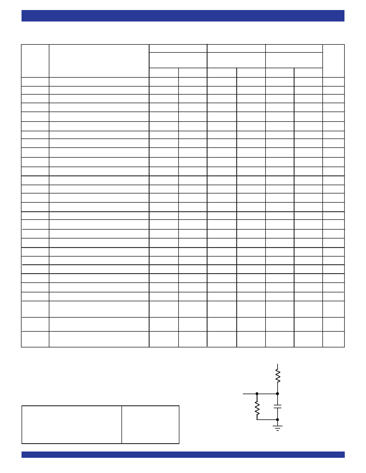
3.3V
330Ω
AC TEST CONDITIONS
Input Pulse Levels
Input Rise/Fall Times
Input Timing Reference Levels
Output Reference Levels
Output Load
GND to 3.0V
3ns
1.5V
1.5V
See Figure 2
6
D.U.T.
510Ω
30pF*
4512 drw 04
Figure 2. Output Load
* Includes jig and scope capacitances.
Share Link: 