24AA00 Ver la hoja de datos (PDF) - Unspecified
Número de pieza
componentes Descripción
Fabricante
24AA00 Datasheet PDF : 19 Pages
| |||
24AA00/24LC00/24C00
1.0 ELECTRICAL CHARACTERISTICS
Absolute Maximum Ratings(†)
VCC.............................................................................................................................................................................6.5V
All inputs and outputs w.r.t. VSS ......................................................................................................... -0.6V to VCC +1.0V
Storage temperature ...............................................................................................................................-65°C to +150°C
Ambient temperature with power applied ................................................................................................-65°C to +125°C
ESD protection on all pins ..........................................................................................................................................4 kV
† NOTICE: Stresses above those listed under “Absolute Maximum Ratings” may cause permanent damage to
the device. This is a stress rating only and functional operation of the device at those or any other conditions
above those indicated in the operational listings of this specification is not implied. Exposure to maximum rating
conditions for extended periods may affect device reliability.
TABLE 1-1: DC CHARACTERISTICS
All Parameters apply across the
Commercial (C): TA = 0°C to +70°C, VCC = 1.8V to 5.5V
recommended operating ranges unless Industrial (I):
TA = -40°C to +85°C, VCC = 1.8V to 5.5V
otherwise noted
Automotive (E) TA = -40°C to +125°C, VCC = 4.5V to 5.5V
Parameter
Symbol
Min.
Max. Units
Conditions
SCL and SDA pins:
High-level input voltage
Low-level input voltage
Hysteresis of Schmitt Trigger
inputs
Low-level output voltage
VIH
VIL
VHYS
VOL
0.7 VCC
.05 VCC
0.3 VCC
—
0.4
Input leakage current
ILI
—
±1
Output leakage current
ILO
—
±1
Pin capacitance (all inputs/outputs)
CIN,
COUT
—
10
Operating current
ICC Write
—
2
ICC Read
—
1
Standby current
ICCS
—
1
Note: This parameter is periodically sampled and not 100% tested.
V (Note)
V (Note)
V VCC ≥ 2.5V (Note)
V IOL = 3.0 mA, VCC = 4.5V
IOL = 2.1 mA, VCC = 2.5V
µA VIN = VCC or VSS
µA VOUT = VCC or VSS
pF VCC = 5.0V (Note)
TA = 25°C, f = 1 MHz
mA VCC = 5.5V, SCL = 400 kHz
mA VCC = 5.5V, SCL = 400 kHz
µA VCC = 5.5V, SDA = SCL = VCC
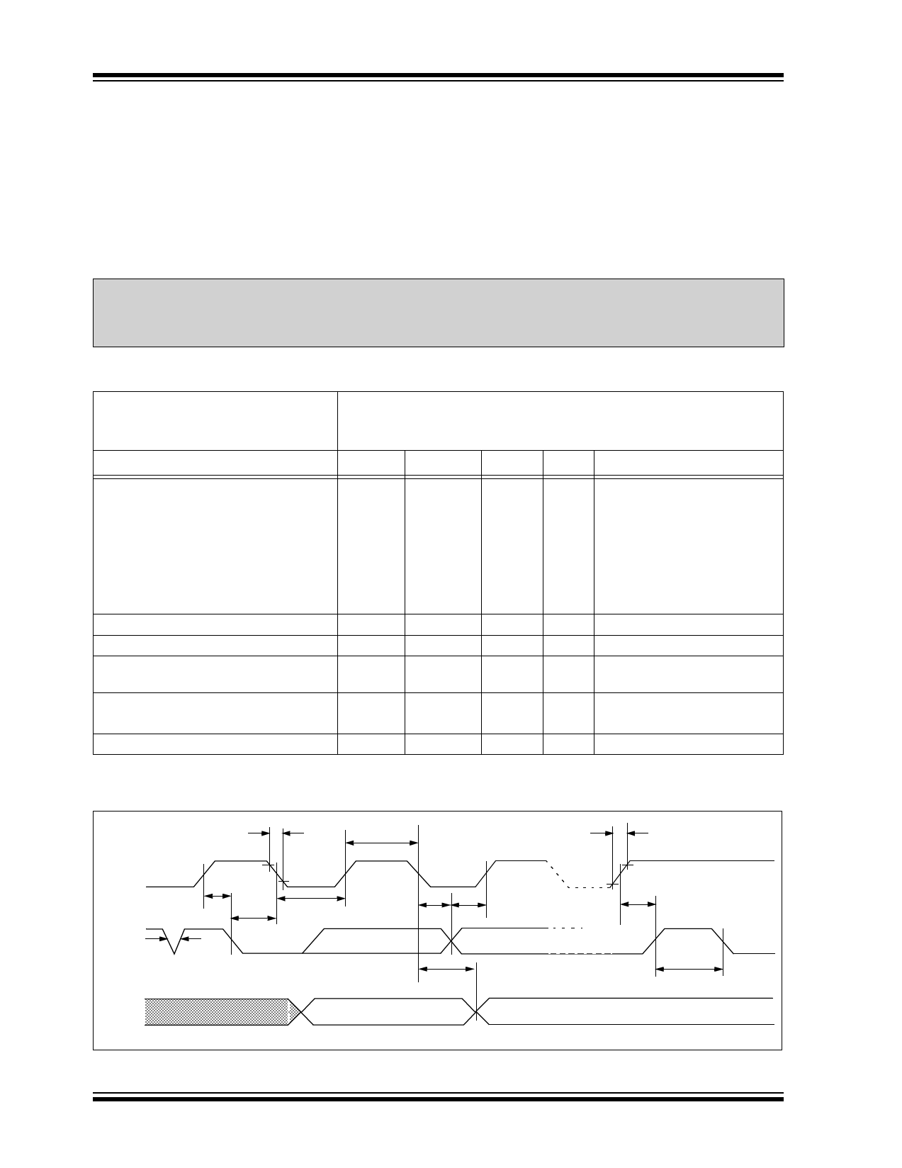
FIGURE 1-1:
BUS TIMING DATA
THIGH
TF
TR
SCL
SDA
IN
SDA
OUT
TSU:STA
TLOW
TSP THD:STA
THD:DAT
TSU:DAT
TSU:STO
TAA
TBUF
DS21178D-page 2
2003 Microchip Technology Inc.
Share Link: 