ZXLD1374 Ver la hoja de datos (PDF) - Diodes Incorporated.
Número de pieza
componentes Descripción
Fabricante
ZXLD1374
Diodes Incorporated.

ZXLD1374 Datasheet PDF : 39 Pages
| |||
A Product Line of
Diodes Incorporated
ZXLD1374
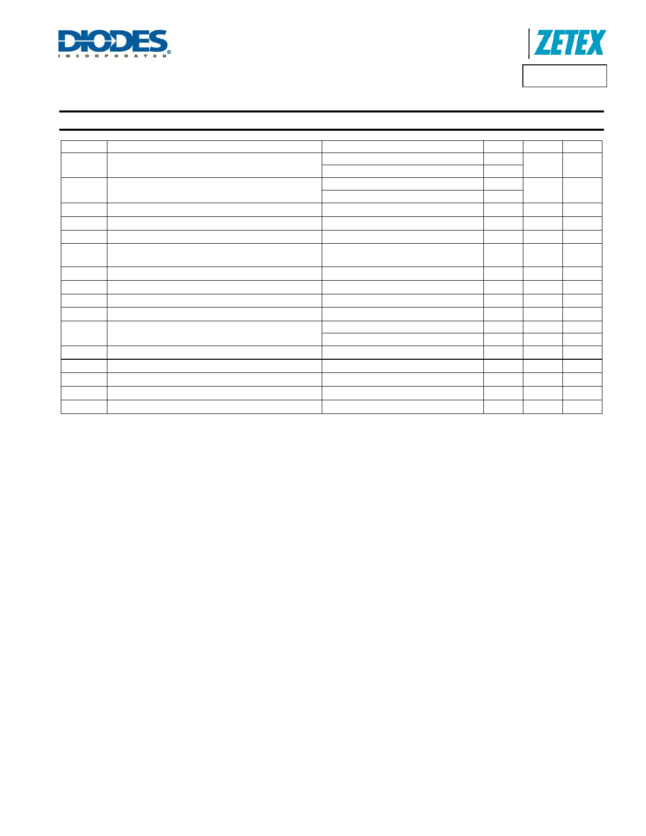
Recommended Operating Conditions (@TA = +25°C, unless otherwise specified.)
Symbol
Parameter
VIN Input Supply Voltage Range
VAUX Auxiliary Supply Voltage Range (Note 8)
Performance/Comment
Min
Max
Unit
Normal operation
8
60
V
Reduced performance operation (Note 7) 6.3
Normal operation
8
60
V
Reduced performance operation (Note 7) 6.3
VSENSE
VLX
ILX
VADJ
Differential Input Voltage
Low Side Switch Output Voltage
Low Side Switch Continuous Output Current
External DC Control Voltage Applied to ADJ Pin to
Adjust Output Current
VVIN-VISM, with 0 ≤ VADJ ≤ 2.5
DC brightness control mode
from 10% to 200%
0
450
mV
60
V
1.5
A
0.125
2.5
V
ISTATUS
IREF
fSW
VTADJ
Status Pin Output Current
Reference External Load Current
Recommended Switching Frequency Range (Note 9)
Temperature Adjustment (TADJ) Input Voltage Range
fPWM Recommended PWM Dimming Frequency Range
REF sourcing current
To maintain 1000:1 resolution
To maintain 200:1 resolution
100
µA
1
mA
300
1000
kHz
0
VREF
V
100
500
Hz
100
1000
Hz
tPWMH/L
VPWMH
VPWML
TJ
GI
PWM Pulse Width in Dimming Mode
PWM Pin High Level Input Voltage
PWM Pin Low Level Input Voltage
Operating Junction Temperature Range
Gain Setting Ratio for Boost and Buck-Boost Modes
PWM input high or low
Ratio= VGI/VADJ
0.005
10
ms
2
5.5
V
0
0.4
V
-40
+125
°C
0.20
0.50
Notes:
7. Device is guaranteed to have started up by 6.5V and as such the minimum applied supply voltage has to be above 6.5V (plus any noise margin).
The ZXLD1374 will, however, continue to function when the input voltage is reduced from ≥ 8V down to 6.3V.
When operating with input voltages below 8V the output current and device parameters may deviate from their normal values; and is dependent on
power MOSFET switch, load and ambient temperature conditions. To ensure best operation in Boost and Buck-boost modes with input voltages, VIN,
between 6.5 and 12V a suitable boot-strap network on VAUX pin is recommended. Performance in Buck mode will be reduced at input voltages (VIN,
VAUX) below 8V. – A boot-strap network cannot be implemented in buck mode.
8. VAUX can be driven from a voltage higher than VIN to provide higher efficiency at low VIN voltages, but to avoid false operation; a voltage should not
be applied to VAUX in the absence of a voltage at VIN.
9. The device contains circuitry to control the switching frequency to approximately 400kHz. The maximum and minimum operating frequency is not
tested.
ZXLD1374
Document number: DS35032 Rev. 3 - 2
5 of 39
www.diodes.com
September 2012
© Diodes Incorporated
Share Link: