ZXLD1320 Ver la hoja de datos (PDF) - Diodes Incorporated.
Número de pieza
componentes Descripción
Fabricante
ZXLD1320
Diodes Incorporated.

ZXLD1320 Datasheet PDF : 18 Pages
| |||
ZXLD1320
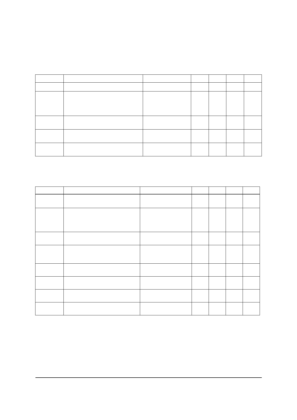
Electrical characteristics (Test conditions: VIN = 4V, TAMB= 25°C unless otherwise stated(a))
DC-DC converter supply parameters
Symbol
VIN
Iq
ISTBY
VREF
TCO(REF)
Parameter
Conditions
Min
Supply voltage
Normal operation 4.0
Quiescent current
Measured into VIN
ADJ pin floating.
(Excluding switch
base current).
Standby current
Measured into VIN.
ADJ pin grounded
Internal reference voltage
ADJ pin floating
480
2.0V<VIN<18V
Internal reference temperature
coefficient.
Typ Max Units
18
V
1.5
mA
12 20 µA
500 520 mV
50
ppm
/K
NOTES:
(a) Production testing of the device is performed at 25°C. Functional operation of the device and parameters specified from -40°C to
+125° Care guaranteed by design, characterisation and process control.
DC-DC converter input parameters
Symbol Parameter
Conditions
Min Typ Max Units
VSENSE
Peak switch current sense
voltage
Measured on ISENSE 45 55 65 mV
pin CFB pin at 0V
ISENSE
Sense input current
Measured into
-15 -7
ISENSE with pin at
0V.
CFB pin at 0V
-1 µA
CFB
Control loop compensation
capacitor
10
nF
VADJ
External dc control voltage
DC brightness
50
applied to ADJ pin to adjust control mode
output current
500 mV
VADJ(th)
Switching threshold of ADJ pin Standby state to
normal operation
26 28 30 mV
TCO(VADJ) Temperature coefficient of
VADJ(th)
+0.3
%/K
RADJ
Internal resistor between VREF VADJ<500mV
and ADJ
100
kΩ
VADJ(clmp) Internal clamp voltage on ADJ 100µA injected into
575
mV
pin
ADJ pin
Issue 1 - January 2008
5
© Zetex Semiconductors plc 2008
www.zetex.com
Share Link: