ZXLD1322DCTC Ver la hoja de datos (PDF) - Zetex => Diodes
Número de pieza
componentes Descripción
Fabricante
ZXLD1322DCTC
Zetex => Diodes

ZXLD1322DCTC Datasheet PDF : 18 Pages
| |||
ZXLD1322
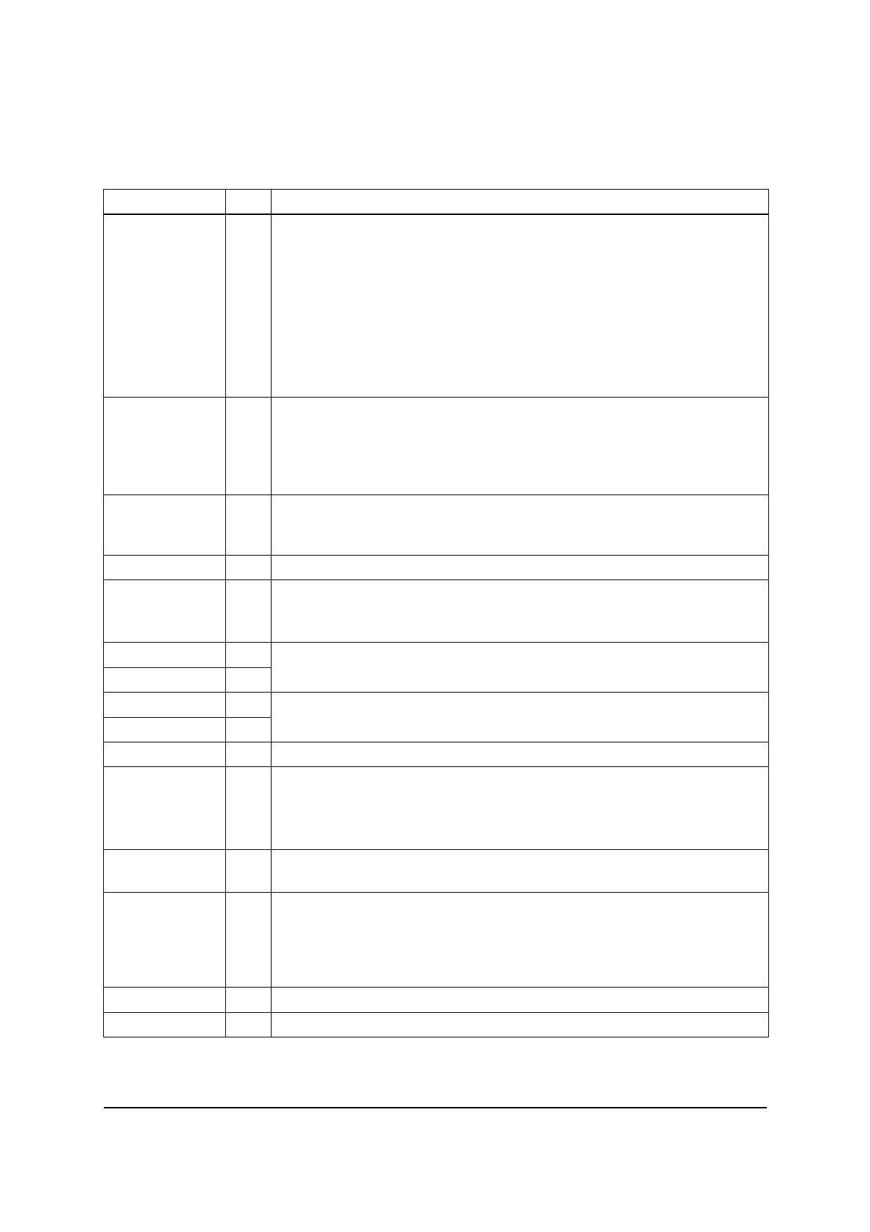
Pin description
Name
ADJ
BIAS
CFB
N/C
ISENSE
EMITTER1
EMITTER2
COLLECTOR2
COLLECTOR1
N/C
M_VIN
VIN
TADJ
VREF
Exposed pad
Pin # Description
1 Adjust input
• Leave floating, or connect to VREF to set 100% output current.
• Drive with dc voltage. (50mV<VADJ< VREF) to adjust output
current from 10% to 100% of set value. (DC brightness control
mode)
• Drive with low frequency (200Hz) PWM control signal to gate
output ‘on’ and ‘off’ at the PWM frequency. (PWM brightness
control mode)
• Drive with low level dc voltage (VADJ<28mV) to turn off device
(Standby mode)
2 Bias pin for setting base current of internal switch transistor
• Short pin to ground to define maximum base drive current for
output switch (Maximum output current condition)
• Connect resistor (RBIAS) from this pin to ground to reduce base
drive current (Reduced output current condition)
3 Control input/output for feedback control loop
• Connect 10nF capacitor from this pin to ground to provide loop
compensation
4 Not connected internally (Open circuit)
5 Switch peak current sense pin
• Connect resistor (Rsense) from this pin to ground to define peak
switch current (ISWPEAK)=0.05/RS
6
7
Switch emitters (Connect both pins to top of RSENSE to sense emitter current)
8
9
Switch Collectors (Connect both pins to lower side of coil)
10 Internally connected - Do not connect to external circuitry
11 Input supply to high side current monitor
• Connect output voltage (whichever is higher)
• Connect resistor (RM) from this pin to to VIN to define nominal
average output (LED) current of 0.1/RM
12 Input supply voltage and load side input of high side current monitor.
Connect to sensing resistor RM.
13 Temperature Adjust input for LED thermal compensation
• Connect thermistor/resistor network to this pin to reduce output
current above a preset temperature threshold.
• Connect to VREF to disable thermal compensation function
(see section on temperature control for details)
14 Internal 0.5V reference voltage output
15 Connect to ground (0V)
Issue 1 - January 2008
4
© Zetex Semiconductors plc 2008
www.zetex.com
Share Link: