ZXLD1320 Ver la hoja de datos (PDF) - Zetex => Diodes
Número de pieza
componentes Descripción
Fabricante
ZXLD1320
Zetex => Diodes

ZXLD1320 Datasheet PDF : 18 Pages
| |||
ZXLD1320
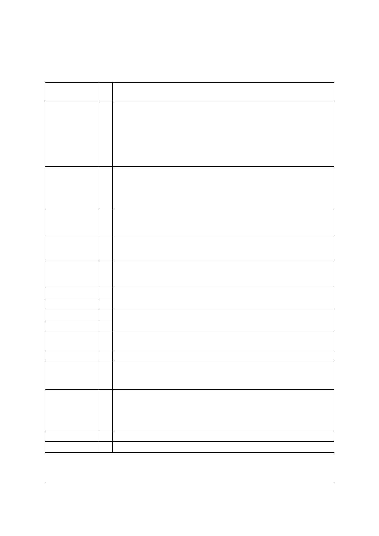
Pin description
Name
ADJ
BIAS
CFB
POK
ISENSE
EMITTER1
EMITTER2
COLLECTOR2
COLLECTOR1
M_LOAD
N/C
VIN
TADJ
VREF
Exposed Pad
Pin Description
#
1 Adjust input
• Leave floating, or connect to VREF to set 100% output current.
• Drive with dc voltage. (50mV<VADJ< VREF) to adjust output current
from 10% to 100% of set value. (DC brightness control mode)
• Drive with low frequency (200Hz) PWM control signal to gate output
‘on’ and ‘off’ at the PWM frequency. (PWM brightness control mode)
• Drive with low level dc voltage (VADJ<28mV) to turn off device
(Standby mode)
2 Bias pin for setting base current of internal switch transistor
• Short pin to ground to define maximum base drive current for
output switch (Maximum output current condition)
• Connect resistor (RBIAS) from this pin to ground to reduce base
drive current (Reduced output current condition)
3 Control input/output for feedback control loop
• Connect 10nF capacitor from this pin to ground to provide loop
compensation
4 Power OK flag output
• Pin is high during normal operation.
• Pin switches low if the switch remains on for more than 500µs (nom)
5 Switch peak current sense pin
• Connect resistor (Rsense) from this pin to ground to define peak
switch current (ISWPEAK)=0.05/RS
6
7 Switch emitters (Connect both pins to top of RSENSE to sense emitter current)
8
9 Switch Collectors (Connect both pins to lower side of coil)
10 Load side input of high side current monitor.
Connect to sensing resistor RM.
11 Not connected locally
12 Positive supply to device (4-18V) and sensing resistor RM
• Decouple to ground with capacitor close to device
• nominal average output (LED) current = 0.1/RM
13 Temperature Adjust input for LED thermal compensation
• Connect thermistor/resistor network to this pin to reduce output
current above a preset temperature threshold.
• Connect to VREF to disable thermal compensation function
(see section on temperature control for details)
14 Internal 0.5V reference voltage output
15 Connect to Ground (0V)
Issue 1 - January 2008
4
© Zetex Semiconductors plc 2008
www.zetex.com
Share Link: