ZPSD211RN Ver la hoja de datos (PDF) - STMicroelectronics
Número de pieza
componentes Descripción
Fabricante
ZPSD211RN Datasheet PDF : 51 Pages
| |||
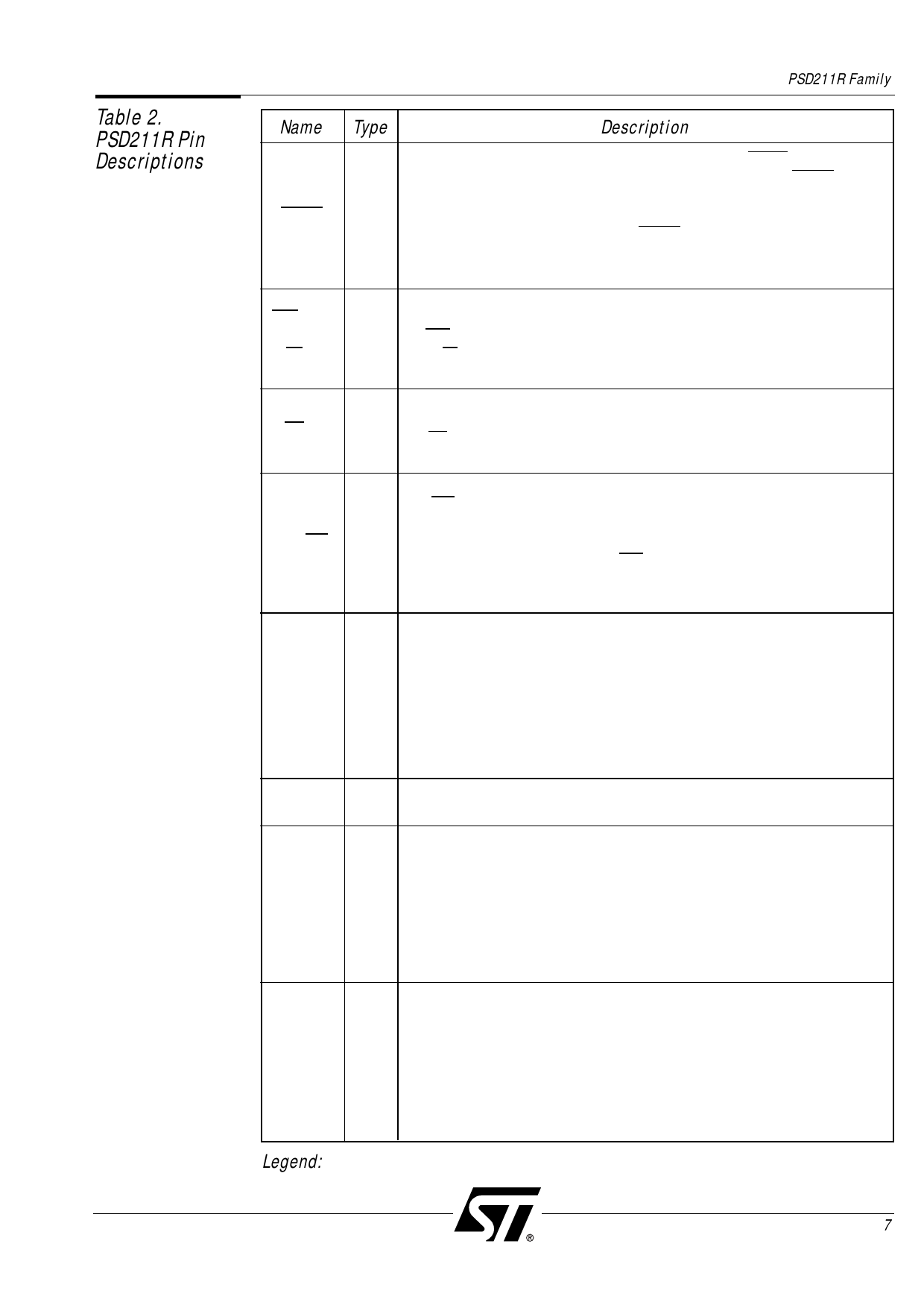
Table 2.
PSD211R Pin
Descriptions
PSD211R Family
Name Type
Description
PSEN
This pin is for 8031 or compatible MCUs that use PSEN to
separate program space from data space. In this case, PSEN is
used for reads from the EPROM.
I Notes:
1) If your MCU does not output a PSEN signal, pull up this pin to
VCC.
2) In programming mode, this pin is pulsed between VPP and 0 V.
The following control signals can be connected to this port, based on
WR/VPP
or
your MCU (and the way you configure the PSD in PSDsoft):
I 1. WR—active-low write pulse.
R/W/VPP
2. R/W—active-high read/active-low write input.
Note: in programming mode, this pin must be tied to VPP.
RD/E
The following control signals can be connected to this port, based on
I
your MCU (and the way you configure the PSD in PSDsoft):
1. RD—active-low read input.
2. E—E clock input.
A19/CSI
The following control signals can be connected to this port:
1. CSI-Active-low chip select input. If your MCU supports a chip
select output, and you want the PSD to save power when not
I
selected, use this pin as a chip select input.
2. If you don’t wish to use the CSI feature, you may use this pin as
an additional input (logic or address) to the PAD. A19 can be
latched with ALE/AS, or be a transparent logic input.
Reset
PSD211R/ZPSD211R:
This pin is user-programmable and can be configured to reset on a
high- or low-level input. Reset must be applied for at least 100 ns.
I ZPSD211RV:
This pin is not configurable, and the chip will only reset on an
active-low level input. Reset must be applied for at least 500 ns,
and no operations may take place for an additional 500 ns minimum.
(See Figure 8.)
ALE/AS
I
Connect ALE or AS to this pin. The polarity of this pin is configurable.
The trailing edge of ALE/AS latches all multiplexed address inputs.
PA0
PA1
PA2
PA3
PA4
PA5
PA6
These pins make up Port A. These port pins are configurable, and
can have the following functions: (see Figure 5)
I/O 1. MCU I/O—in this mode, the direction of the pin is defined by its
direction bit, which resides in the direction register.
2. Latched address output.
PA7
PB0
PB1
PB2
PB3
PB4
PB5
PB6
PB7
These pins make up Port B. These port pins are configurable, and
can have the following functions: (see Figure 6)
1. MCU I/O —in this mode, the direction of the pin is defined by its
I/O
direction bit, which resides in the direction register.
2. Chip select output —each of PB0-3 has four product terms
available per pin, while PB4-7 have 2 product terms each.
See Figure 4.
Legend: The Type column abbreviations are: I = input only; I/O = input/output; P = power.
7
Share Link: 