XM28C020 Ver la hoja de datos (PDF) - Xicor -> Intersil
Número de pieza
componentes Descripción
Fabricante
XM28C020 Datasheet PDF : 16 Pages
| |||
XM28C020
ABSOLUTE MAXIMUM RATINGS*
Temperature under Bias .................. –65°C to +135°C
Storage Temperature ....................... –65°C to +150°C
Voltage on any Pin with
Respect to VSS ................................................ –1V to +7V
D.C. Output Current ............................................. 5mA
Lead Temperature
(Soldering, 10 seconds) .............................. 300°C
*COMMENT
Stresses above those listed under “Absolute Maximum
Ratings” may cause permanent damage to the device.
This is a stress rating only and the functional operation of
the device at these or any other conditions above those
indicated in the operational sections of this specification is
not implied. Exposure to absolute maximum rating condi-
tions for extended periods may affect device reliability.
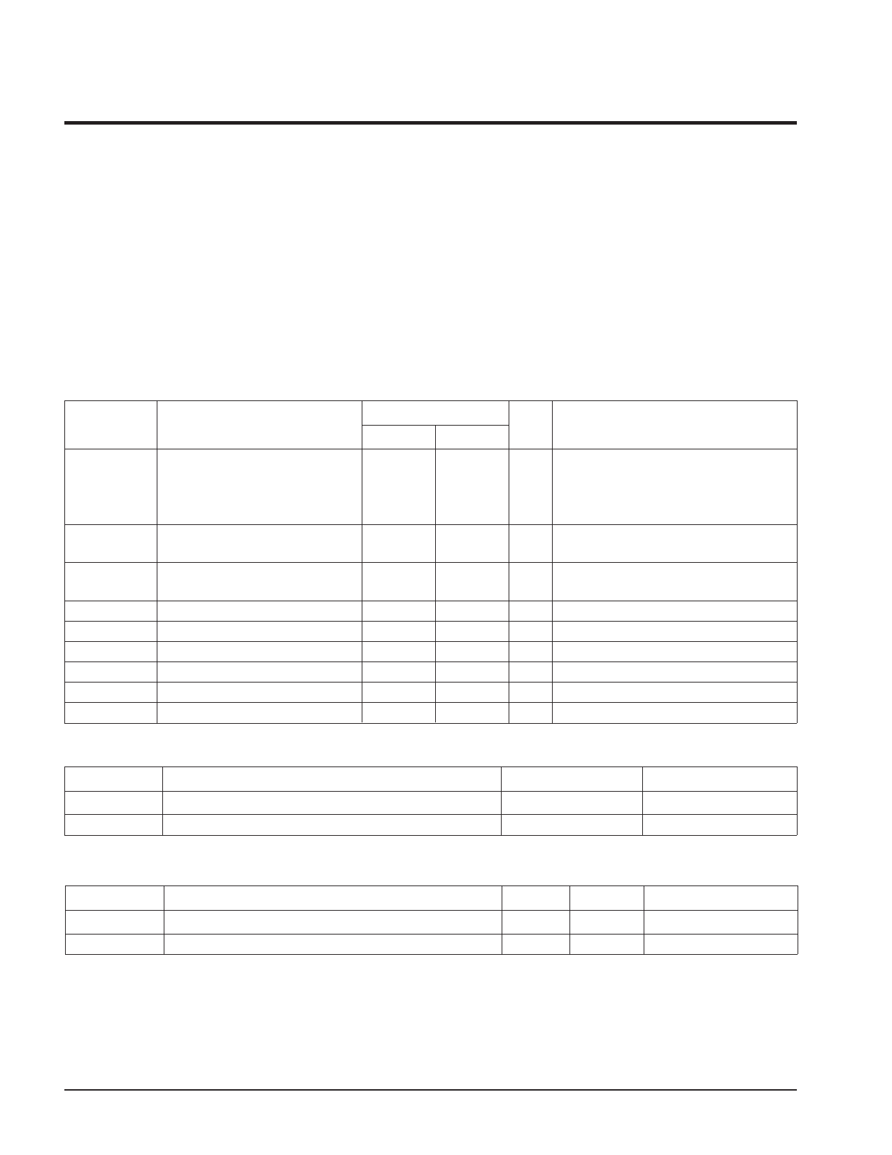
D.C. OPERATING CHARACTERISTICS
XM28C020 TA = 0°C to +70°C, VCC = +5V ±10%, unless otherwise specified.
XM28C020I TA = –40°C to +85°C, VCC = +5V ±10%, unless otherwise specified.
XM28C020M TA = –55°C to +125°C, VCC = +5V ±10%, unless otherwise specified.
Limits
Symbol
Parameter
Min.
Max. Units
Test Conditions
ICC
VCC Current (Active)
(TTL Inputs)
100
mA CE = OE = VIL, WE = VIH,
All I/O’s = Open, 1 Device Active
Address Inputs = TTL Levels
@ f = 5MHz
ISB1
VCC Current (Standby)
(TTL Inputs)
25
mA CE = VIH, OE = VIL
All I/O’s = Open, Other Inputs = VIH
ISB2
VCC Current (Standby)
(CMOS Inputs)
5
mA CE = VIH, OE = VIL
All I/O’s = Open, Other Inputs = VCC
ILI
Input Leakage Current
20
µA VIN = VSS to VCC
ILO
Output Leakage Current
20
µA VOUT = VSS to VCC, CE = VIH
VlL
Input LOW Voltage
–1
0.8
V
VIH
Input HIGH Voltage
2
VCC + 1 V
VOL
Output LOW Voltage
0.4
V IOL = 2.1mA
VOH
Output HIGH Voltage
2.4
V IOH = –400µA
3856 PGM T02.2
POWER-UP TIMING
Symbol
Parameter
Typ.(1)
Units
tPUR(2)
Power-up to Initiation of Read Operation
100
tPUW(2)
Power-up to Initiation of Write Operation
5
µs
ms
3872 PGM T03
CAPACITANCE TA = +25°C, f = 1MHz, VCC = 5V
Symbol
Parameter
CI/O(2)
CIN(2)
Input/Output Capacitance
Input Capacitance
Max.
50
50
Units
pF
pF
Test Conditions
VI/O = 0V
VIN = 0V
3872 PGM T04.1
Notes: (1) Typical values are for TA = 25°C and nominal supply voltage.
(2) This parameter is periodically sampled and not 100% tested.
10
Share Link: 