L2340 Ver la hoja de datos (PDF) - LOGIC Devices
Número de pieza
componentes Descripción
Fabricante
L2340 Datasheet PDF : 11 Pages
| |||
DEVICES INCORPORATED
L2340
Digital Synthesizer
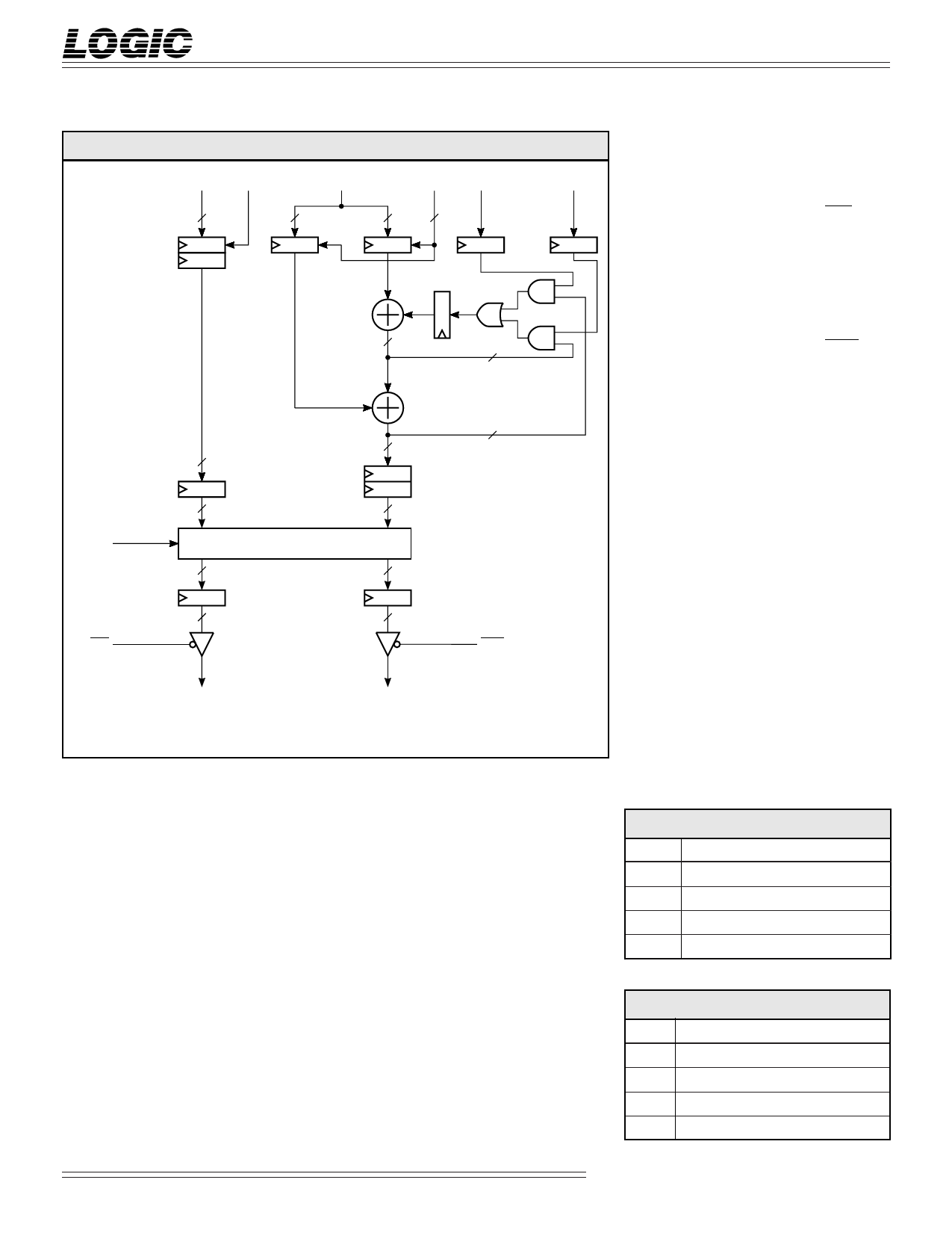
L2340 FUNCTIONAL BLOCK DIAGRAM
AM14-0 ENA
PH31-0
ENP1-0 FM
15
32
32
2
M
C
AM
Outputs
I15-0 — x-coordinate Data Output
PM
I15-0 is the 16-bit Cartesian x-coordi-
nate Data output port. When OEI is
HIGH, I15-0 is forced into the high-
impedance state. I15 is forced HIGH if
OBIQ is LOW.
Q15-0 — y-coordinate Data Output
OBIQ
OEI
32
PM
32
FM
32
24
15
15
24
* TRANSFORM
PROCESSOR
16
16
16
16
OEQ
Q15-0 is the 16-bit Cartesian y-coordi-
nate Data output port. When OEQ is
HIGH, Q15-0 is forced into the high-
impedance state. Q15 is forced HIGH
if OBIQ is LOW.
Controls
ENA — Amplitude Modulation Data
Input Enable
When ENA is HIGH, AM is latched
into the input register on the rising
edge of clock. When ENA is LOW, the
value stored in the register is un-
changed.
ENP1-0 — Phase Modulation Data Input
Control
I15-0
Q15-0
* REQUIRES 18 CYCLES TO COMPLETE AND IS FULLY PIPELINED
SIGNAL DEFINITIONS
Inputs
ENP1-0 is the 2-bit Phase Modulation
Data Input Control that determines
one of the four modes shown in Table
1. ‘M’ is the Modulation Register and
‘C’ is the Carrier Register as shown in
the Functional Block Diagram.
Power
Vcc and GND
+5V power supply. All pins must be
connected.
Clock
CLK — Master Clock
The rising edge of CLK strobes all
enabled registers.
AM14-0 — Amplitude Modulation Data
Input
AM14-0 is the 15-bit Amplitude
Modulation Data input port. AM14-0
is latched on the rising edge of CLK.
PH31-0 — Phase Angle Data Input
PH31-0 is the 32-bit Phase Angle Data
input port. Input phase accumulators
are loaded through this port into
registers enabled by ENP1-0. PH31-0 is
latched on the rising edge of CLK.
TABLE 1. REGISTER OPERATION
ENP1-0 Configuration
0 0 No registers enabled, current data held
0 1 M register input enabled, C data held
1 0 C register input enabled, M data held
1 1 M register = 0, C register input enabled
TABLE 2. ACCUMULATOR CONTROL
FM PM Configuration
0 0 No accumulation (normal operation)
0 1 PM accumulator path enabled
1 0 FM accumulator path enabled
1 1 Logical OR of PM and FM (Nonsensical)
Special Arithmetic Functions
2
08/16/2000–LDS.2340-E
Share Link: 