HSP50016 Ver la hoja de datos (PDF) - Intersil
Número de pieza
componentes Descripción
Fabricante
HSP50016 Datasheet PDF : 31 Pages
| |||
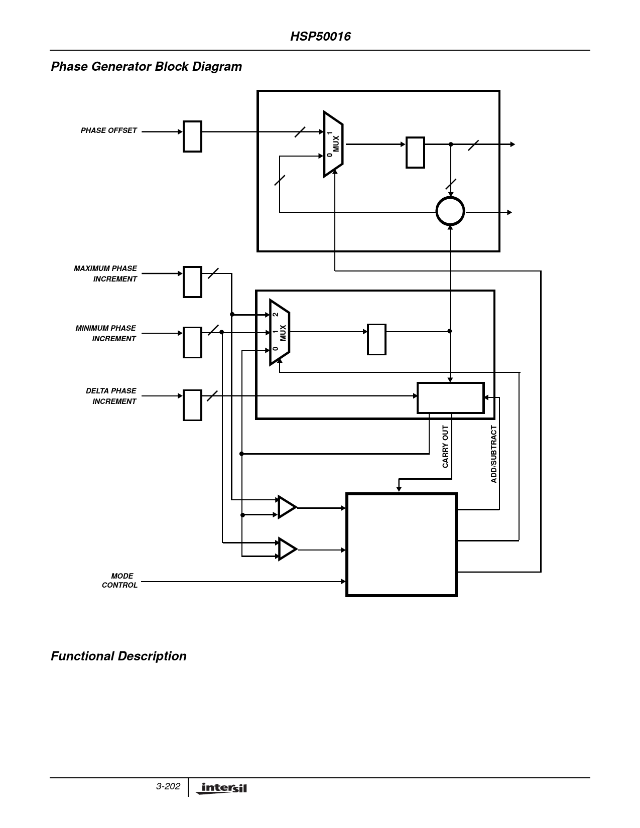
Phase Generator Block Diagram
HSP50016
PHASE ACCUMULATOR
†PHASE OFFSET
R
E
>G
18
33
PHASE REGISTER
R
E
18
>G
33
+
+
-
PHASE WORD
(TO THE
SIN/COS
GENERATOR)
PHASE ADDER
CARRY OUT
†MAXIMUM PHASE
INCREMENT
†MINIMUM PHASE
INCREMENT
†DELTA PHASE
INCREMENT
32
R
E
>G
32
R
E
>G
R 32
E
>G
MUX SELECT 1
PHASE INCREMENT ACCUMULATOR
PHASE
INCREMENT
REGISTER
R
E
>G
MUX SELECT 0
ADDER /
SUBTRACTOR
INITIALIZE
PHASE INCR.
TO MIN
≤
INITIALIZE
PHASE INCR.
TO MAX
>
CONTROL
†MODE
CONTROL
† Indicates parameters set in Control Registers.
FIGURE 2. PHASE GENERATOR BLOCK DIAGRAM
MUX SELECT 0
MUX SELECT 1
Functional Description
The primary function of the DDC is to extract a narrow
frequency band of interest from a wideband input, convert that
band to baseband and output it in either a quadrature or real
form. This narrow band extraction is accomplished by down
converting and centering the band of interest at DC. The
conversion is done by multiplying the input data with a
quadrature sinusoid. A quadrature lowpass filter is applied to
3-202
the multiplier outputs. Identical real lowpass filters are
provided in the in-phase (I) and quadrature phase (Q)
processing branches. Each filtering chain consists of a
cascaded HDF and FIR filter, which extracts the band of
interest. During filtering, the signal is decimated by a rate
which is proportional to the output bandwidth. The bandwidth
of the resulting signal is the double sided passband width of
the lowpass filters. An Output Formatter manipulates the filter
output to provide the data in a variety of serial data formats.
Share Link: 