XC9103 Ver la hoja de datos (PDF) - TOREX SEMICONDUCTOR
Número de pieza
componentes Descripción
Fabricante
XC9103 Datasheet PDF : 19 Pages
| |||
XC9103/04/05 Series
Ceramic Cap. Compatible Step-Up DC/DC Converters
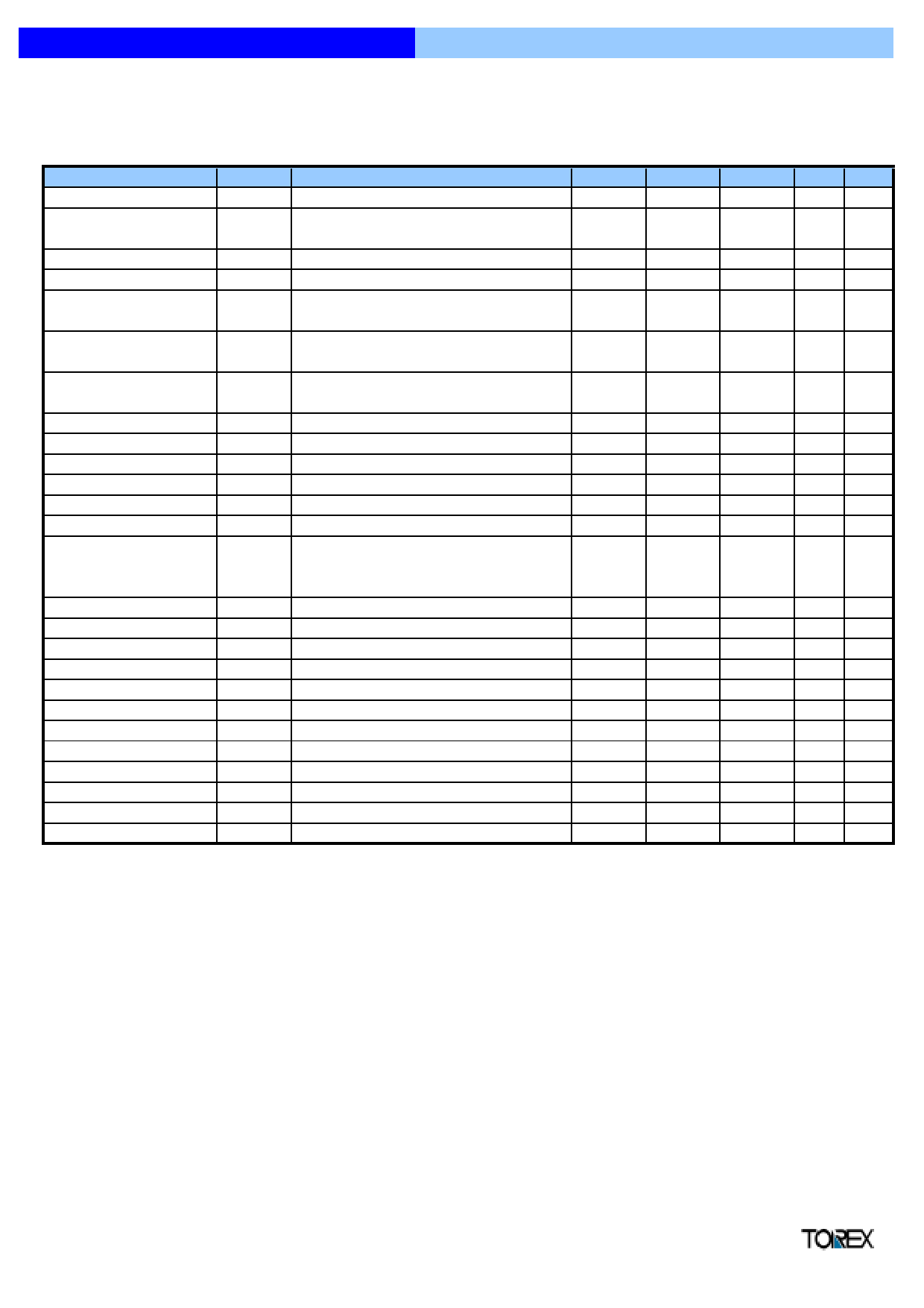
" ELECTRICAL CHARACTERISTICS
XC9103B092MR, XC9104B092MR, XC9105B092MR
XC9103D092MR, XC9104D092MR, XC9105D092MR
(FOSC=180 (kHz)
PARAMETER
SYMBOL
CONDITIONS
MIN.
TYP.
Output Voltage
Output Voltage Range
VOUT
VOUTSET
VIN=VOUTSET× 0.6, VDD=3.3V
IOUT=10mA, Using 2SD1628
3.234
1.5
3.300
-
FB Control Voltage
VFB
0.882
0.900
*1 Power Supply Voltage Range VDD
1.8
-
Operation Start Voltage
VST1
Recommended Circuit using 2SD1628,
-
-
IOUT=1.0mA
*1
Oscillation Start Voltage
VST2
No external connections
-
-
CE connected to VDD, Voltage applied, FB=0V
Operation Holding Voltage
VHLD
Recommended Circuit using 2SD1628,
-
-
IOUT=1.0mA
Supply Current 1
IDD1
Same as VST2, VDD=3.300V
-
45
Supply Current 2
IDD2
Same as IDD1, FB=1.2V
-
17
Stand-by Current
ISTB
Same as IDD1, CE=0V
-
-
Oscillation Frequency
FOSC
Same as IDD1
153
180
Maximum Duty Ratio
MAXDTY
Same as IDD1
75
81
PWM Duty Ratio
PFMDTY
No Load (XC9104B/D, 9105B/D)
20
28
*3
Step input to FB ( Pulse width:2.0µS or more)
Overcurrent SENSE Voltage VLMT
EXT = Low level voltage
170
250
(XC9103B, 9104B, 9105B)
Efficiency
EFFI
Recommended Circuit using XP161A1355
85
Soft-start Time
TSS
5.0
10.0
CE "High" Voltage
VCEH
Same as IDD1
0.65
-
CE "Low" Voltage
VCEL
Same as IDD1
-
-
*2
PWM "High" Voltage
VPWMH
IOUT=1.0mA
(XC9105B/D)
VDD - 0.2
-
*2
PWM "Low" Voltage
VPWML
IOUT=1.0mA
(XC9105B/D)
-
EXT "High" ON Resistance REXTH
Same as IDD1, VEXT=VOUT-0.4V
-
24
EXT "Low" ON Resistance REXTL
Same as IDD1, VEXT=0.4V
-
16
CE "High" Current
ICEH
Same as IDD2, CE=VDD
-
-
CE "Low" Current
ICEL
Same as IDD2, CE=0V
-
-
FB "High" Current
FB "Low" Current
IFBH
IFBL
Same as IDD2, FB=VDD
Same as IDD2, FB=0V
-
-
-
-
Test Conditions: Unless otherwise stated, CL: ceramic capacitor, recommended MOS FET should be connected.
VOUT=3.30 (V), VIN=2.00 (V), IOUT=170 (mA)
MAX.
3.366
30.0
0.918
10
0.9
Ta=25OC
UNITS CIRCUIT
V
1
V
2
V
4
V
-
V
3
0.8
V
4
0.7
V
3
64
µA
4
24
µA
4
1.0
µA
5
207
kHz
4
87
%
4
36
%
1
330
mV
6
%
1
20.0
mS
1
-
V
5
0.20
V
5
V
1
VDD - 1.0 V
1
36
Ω
4
24
Ω
4
0.1
µA
5
-0.1
µA
5
0.1
µA
5
-0.1
µA
5
" NOTES
*1 Although the IC starts step-up operations from a VDD of 0.8V, the output voltage and oscillation frequency are stabilized at
VDD ≥ 1.8V. Therefore, a VDD of more than 1.8V is recommended when VDD is supplied from VIN or other power sources.
*2 With the XC9105 series, the CE pin also serves as a PWM/PFM switching pin. In operation, PWM control is selected when the voltage at the CE pin is
more than VDD -0.2V. On the other hand, PWM/PFM automatic switching control at a duty = 25% is selected when the voltage at the CE pin is less than
VDD -1.0V and more than VCEH.
*3 The overcurrent limit circuit of this IC is designed to monitor the ripple voltage so please select your external components carefully to prevent VLMT
being reached under low temperature conditions as well as normal operating conditions. Following current limiter circuit operations, which in turn causes
the IC's operations to stop, the operations of the IC can be returned to normal with a toggle of the CE pin or by turning the power supply back on.
4
Semiconductor Ltd.
Share Link: 