X28C010D Ver la hoja de datos (PDF) - Intersil
Número de pieza
componentes Descripción
Fabricante
X28C010D Datasheet PDF : 23 Pages
| |||
X28C010
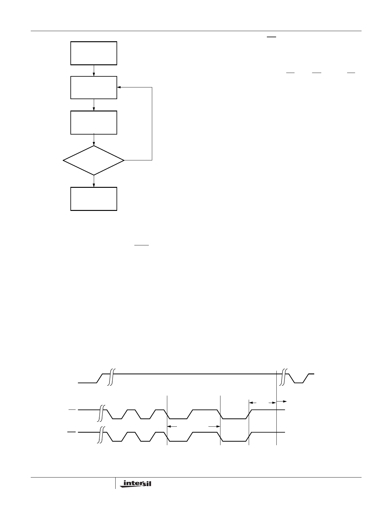
Last Write
Load Accum
From Addr N
Compare
Accum with
Addr N
Compare
No
Ok?
Yes
Ready
FIGURE 5. TOGGLE BIT SOFTWARE FLOW
The Toggle Bit can eliminate the software housekeeping
chore of saving and fetching the last address and data
written to a device in order to implement DATA Polling. This
can be especially helpful in an array comprised of multiple
X28C010 memories that is frequently updated. Toggle Bit
Polling can also provide a method for status checking in
multiprocessor applications. The timing diagram in Figure 4
illustrates the sequence of events on the bus. The software
flow diagram in Figure 5 illustrates a method for polling the
Toggle Bit.
Hardware Data Protection
The X28C010 provides three hardware features that protect
nonvolatile data from inadvertent writes.
• Noise Protection—A WE pulse less than 10ns will not
initiate a write cycle.
• Default VCC Sense—All functions are inhibited when VCC
is ≤ 3.5V.
• Write inhibit—Holding either OE LOW, WE HIGH, or CE
HIGH will prevent an inadvertent write cycle during power-
up and power-down, maintaining data integrity.
Software Data Protection
The X28C010 offers a software controlled data protection
feature. The X28C010 is shipped from Intersil with the
software data protection NOT ENABLED: that is the device
will be in the standard operating mode. In this mode data
should be protected during power-up/-down operations
through the use of external circuits. The host would then
have open read and write access of the device once VCC
was stable.
The X28C010 can be automatically protected during power-
up and power-down without the need for external circuits by
employing the software data protection feature. The internal
software data protection circuit is enabled after the first write
operation utilizing the software algorithm. This circuit is
nonvolatile and will remain set for the life of the device
unless the reset command is issued.
Once the software protection is enabled, the X28C010 is
also protected from inadvertent and accidental writes in the
powered-up state. That is, the software algorithm must be
issued prior to writing additional data to the device.
Software Algorithm
Selecting the software data protection mode requires the
host system to precede data write operations by a series of
three write operations to three specific addresses. Refer to
Figures 6 and 7 for the sequence. The three byte sequence
opens the page write window enabling the host to write from
one to two hundred fifty-six bytes of data. Once the page
load cycle has been completed, the device will automatically
be returned to the data protected state.
Software Data Protection
VCC
0V
Data
Addr
AA
5555
CE
55
2AAA
WE
A0
5555
≤ tBLC MAX
tWC
Writes
Ok
Byte
or
Page
FIGURE 6. TIMING SEQUENCE—BYTE OR PAGE WRITE
(VCC)
Write
Protected
6
FN8105.0
May 11, 2005
Share Link: 