WED2ZL361MV Ver la hoja de datos (PDF) - White Electronic Designs Corporation
Número de pieza
componentes Descripción
Fabricante
WED2ZL361MV Datasheet PDF : 12 Pages
| |||
White Electronic Designs
WED2ZL361MV
FUNCTION DESCRIPTION
The WED2ZL361MV is an NBL SSRAM designed to
sustain 100% bus bandwidth by eliminating turnaround
cycle when there is transition from Read to Write, or vice
versa. All inputs (with the exception of OE#, LBO and ZZ)
are synchronized to rising clock edges.
All read, write and deselect cycles are initiated by the
ADV# input. Subsequent burst addresses can be internally
generated by the burst advance pin (ADV#). ADV# should
be driven to Low once the device has been deselected in
order to load a new address for next operation.
Clock Enable (CKE) pin allows the operation of the chip to
be suspended as long as necessary. When CKE is high,
all synchronous inputs are ignored and the internal device
registers will hold their previous values. NBL SSRAM
latches external address and initiates a cycle when CKE
and ADV are driven low at the rising edge of the clock.
Output Enable (OE) can be used to disable the output at
any given time. Read operation is initiated when at the
rising edge of the clock, the address presented to the
address inputs are latched in the address register, CKE is
driven low, the write enable input signals WE# are driven
high, and ADV# driven low. The internal array is read
between the first rising edge and the second rising edge
of the clock and the data is latched in the output register.
At the second clock edge the data is driven out of the
SRAM. During read operation OE# must be driven low for
the device to drive out the requested data.
Write operation occurs when WE# is driven low at the rising
edge of the clock. BW#[d:a] can be used for byte write
operation. The pipe-lined NBL SSRAM uses a late-late
write cycle to utilize 100% of the bandwidth. At the first
rising edge of the clock, WE# and address are registered,
and the data associated with that address is required two
cycle later.
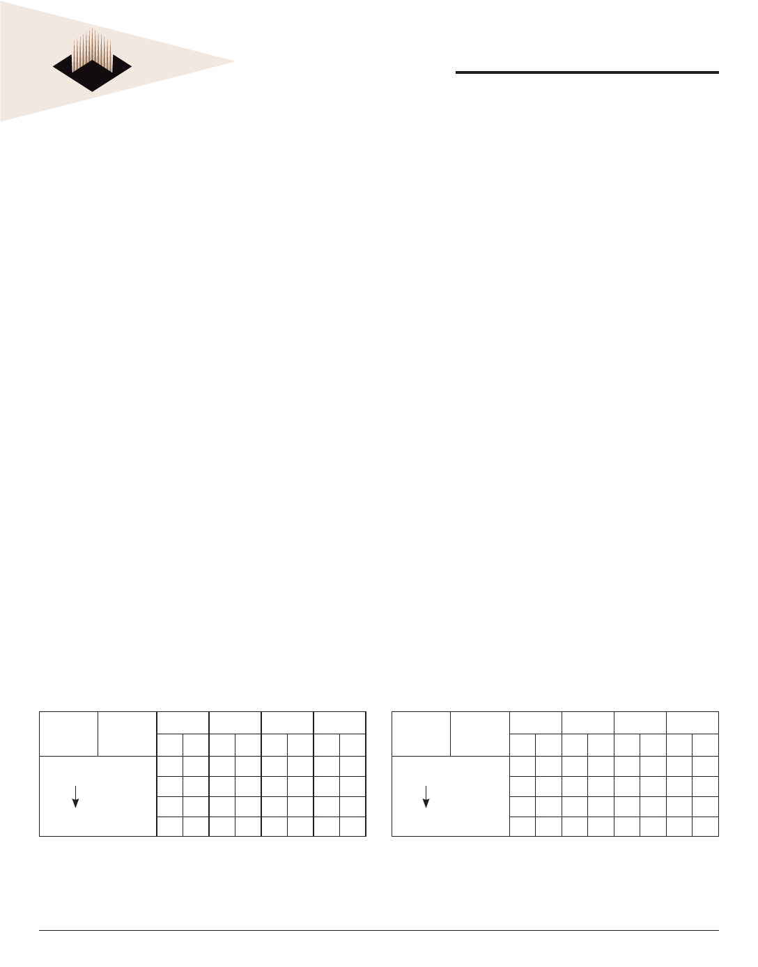
Subsequent addresses are generated by ADV High for
the burst access as shown below. The starting point of the
burst seguence is provided by the external address. The
burst address counter wraps around to its initial state upon
completion. The burst sequence is determined by the state
of the LBO pin. When this pin is low, linear burst sequence
is selected. And when this pin is high, Interleaved burst
sequence is selected.
During normal operation, ZZ must be driven low. When ZZ
is driven high, the SRAM will enter a Power Sleep Mode
after 2 cycles. At this time, internal state of the SRAM is
preserved. When ZZ returns to low, the SRAM operates
after 2 cycles of wake up time.
BURST SEQUENCE TABLE
(Interleaved Burst, LBO = High)
Case 1 Case 2 Case 3 Case 4
LBO Pin High
First Address
A1 A0 A1 A0 A1 A0 A1 A0
00011011
01001110
LBO Pin High
First Address
Fourth Address
10110001
11100100
Fourth Address
(Linear Burst, LBO = Low)
Case 1 Case 2 Case 3 Case 4
A1 A0 A1 A0 A1 A0 A1 A0
00011011
01101100
10110001
11000110
NOTE 1: LBO pin must be tied to High or Low, and Floating State must not be allowed.
June 2004
Rev. 3
2
White Electronic Designs Corporation • (602) 437-1520 • www.wedc.com
Share Link: 