VV6404C001-B2 Ver la hoja de datos (PDF) - STMicroelectronics
Número de pieza
componentes Descripción
Fabricante
VV6404C001-B2 Datasheet PDF : 54 Pages
| |||
VV5404 & VV6404
1. Fast QCK: the falling edge of the clock qualifies the nibble data irrespective of whether it is the most or the least
significant nibble.
2. Slow QCK: the rising edge of the clock qualifies the most significant nibbles while the falling edge of the clock
qualifies the least significant nibbles.
The FST can be enabled/disabled via the serial interface.
OEB tri-states all 4 databus lines, D[3:0], the qualification clock, QCK and the frame start signal, FST.
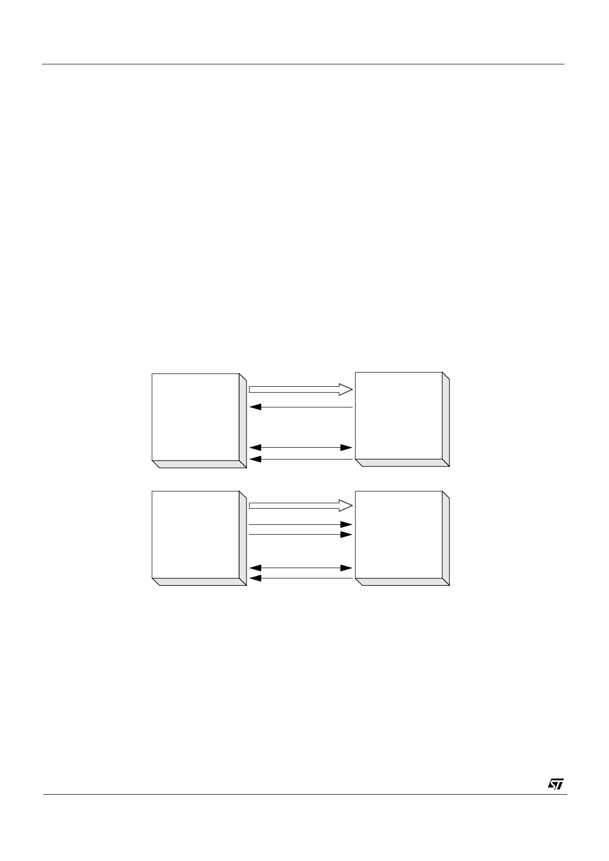
There are 3 main ways of interfacing to the VV5404 or VV6404 sensor based on the above signals:
1. The processor capturing the data (or colour co-processor for VV6404) supplies the sensor clock, CKI, and uses
the embedded control sequences to synchronise with the frame and line level timings. Thus the processor and
sensor are running off derivatives of the same fundamental clock (4 fsc - 14.31818 MHz). To allow the receiver
to determine the best sampling position of the video data, during its power-up sequence the sensor outputs a
101010... sequence on each of its databus lines for the video processor to lock on to.
2. The video processor uses a free-running QCK supplied by the sensor to sample the incoming video data
stream. The embedded control sequences are used to synchronise the frame and line level timings. A crystal is
used to generate the clock for the sensor.
3. The video processor uses FST and the data only mode for QCK to synchronise to the incoming video data. Pri-
marily intended for interfacing to frame grabbers.
The 2-wire serial interface provides complete control over how the sensor is setup and run. Exposure and gain values
are programmed via this interface. Section 5. defines the communications protocol and the register map of all the
locations which can be accessed via the serial interface.
Sensor
D[3:0]
CLKI
SDA
Colour
Co-processor
(processor)
SCL
Sensor
D[3:0]
QCK
FST
SDA
Colour
Co-processor
(processor)
SCL
Figure 2 : Interfacing Options
Using the first two interface options outlined above it is possible to control the sensor and receive video data via a 9-
wire cable between the sensor and the video processor/colour-processor.
1. A 4-wire data bus (D[3:0]) for sending both video data and embedded timing references.
2. A 2-wire serial interface (SDA,SCL).
3. The clock for the sensor or QCK from the sensor.
4. VCC and GND power lines.
The various image read-out and frame rate options are detailed in Sections 2 and 3 respectively.
5/54
CD5404-6404F-A
Share Link: 