VV6404C001-B2 Ver la hoja de datos (PDF) - STMicroelectronics
Número de pieza
componentes Descripción
Fabricante
VV6404C001-B2 Datasheet PDF : 54 Pages
| |||
VV5404 & VV6404
1. Introduction
VV5404 and VV6404 are CIF format CMOS image sensors capable of outputing digital pixel data at frame rates, of
upto 30 frames per second. The VV5404 is a monochrome part, while the VV6404 has a colour filter applied over the
sensor array.
Important: The VV6404 sensor’s video data stream only contains raw colourised pixel data. A colour co-processor
is required to generate for example either a CIF or a QCIF format YUV colour image.
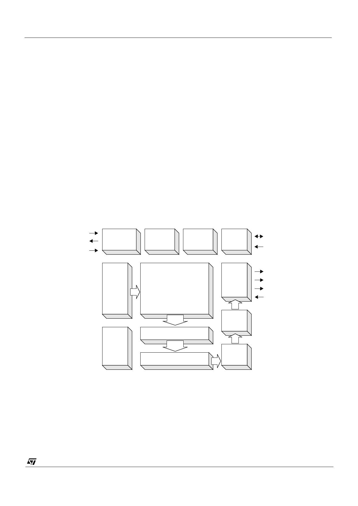
The 356 x 292 pixel sensors have an on-chip 8-bit analogue to digital converter (Figure 1). The sensors offer very
flexible digital interface, the main components of which are listed below:
1. A tri-stateable 4-wire data bus (D[3:0]) for sending both video data and embedded timing references.
2. A data qualification clock, QCK, which can be programmable via the serial interface to behave in a number of
different ways (Tri-stateable).
3. A frame start signal, FST (Tri-stateable).
4. A 2-wire serial interface (SDA,SCL) for controlling and setting up the device.
5. The ability to synchronise the operation of multiple cameras - synchronisation input, SIN.
An 8-bit pixel value is transmitted across the 4 wire tri-stateable databus as series pair of 4-bit nibbles, most significant
nibble first. Along within the pixel data, codes representing the start and end frames and the start and end of lines are
embedded within the video data stream to allow the video processor to synchronise with video data the camera
module is generating. Section 4. defines the format for the output video datastream.
CLKI
CLKO
SIN
BLACK
CALIBRATION
IMAGE
FORMAT
EXPOSURE
REGISTERS
SERIAL
INTER-
FACE
SDA
SCL
VERTICAL
SHIFT
REGISTER
PHOTO DIODE
ARRAY
OUTPUT
FORMAT
D[3:0]
QCK
FST
OEB
ANALOG
VOLTAGE
REFS.
SAMPLE & HOLD
HORIZONTAL SHIFT
REGISTER
8-bit
ADC
GAIN
STAGE
Figure 1 : Block Diagram of VV5404 and VV6404 Image Sensors
To complement the embedded control sequences a data qualification clock, QCK, and a frame start signal are also
available. QCK can be set-up to either be:
1. Disabled
2. Free-running.
3. Qualify only the control sequences and the pixel data.
4. Qualify the pixel data only
There is also the choice of two different QCK frequencies, where one is twice the frequency of the other.
CD5404-6404F-A
4/54
Share Link: 