VSC7938 Ver la hoja de datos (PDF) - Vitesse Semiconductor
Número de pieza
componentes Descripción
Fabricante
VSC7938 Datasheet PDF : 16 Pages
| |||
VITESSE
SEMICONDUCTOR CORPORATION
Preliminary Data Sheet
VSC7938
SONET/SDH 3.125Gb/s
Laser Diode Driver with Automatic Power Control
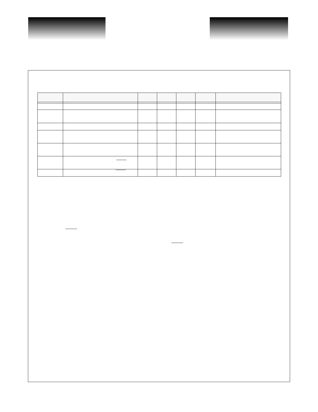
Table 3: PECL and TTL/CMOS Inputs and Outputs Specifications
Symbol
VID
VICM
IIN
VIH
VIL
Parameter
Differential Input Voltage
Common-Mode Input Voltage
Clock and Data Input Current
TTL Input High Voltage
(ENABLE, LATCH)
TTL Input Low Voltage
(ENABLE, LATCH)
TTL Output High Voltage (FAIL)
TTL Output Low Voltage (FAIL)
Min
100
VCC -
1.49
-1
2.0
Typ
VCC -
1.32
Max
1600
VCC -
VID/4
10
Units
Conditions
mVp-p (DATA+)-(DATA-)
V PECL Compatible
µA
V
0.8
2.4
VCC -
0.3
VCC
0.1
0.44
V
V Sourcing 50µA
V Sinking 100µA
Absolute Maximum Ratings(1)
Power Supply Voltage (VCC)............................................................................................................... -0.5V to 6V
Current into BIAS.....................................................................................................................-20mA to +150mA
Current into OUT+, OUT- ...............................................................................................................................TBD
Current into MD .............................................................................................................................-5mA to +5mA
Current into FAIL ......................................................................................................................... -10mA to 30mA
Voltage at DATA+, DATA-, CLK+, CLK-, ENABLE, LATCH......................................... -0.5V to (VCC + 0.5V)
Voltage at APCFILT, MODSET, BIASMAX, APCSET, MD, FAIL, SLWSTRT.......................... -0.5V to +3.0V
Voltage at OUT+, OUT- ..................................................................................................... -0.5V to (VCC + 1.5V)
Voltage at BIAS .................................................................................................................. -0.5V to (VCC + 0.5V)
Continouous Power Dissipation (TA = +85°C, TQFP derate 20.8mW/°C above +85°C) .......................1350mW
Operating Junction Temperature Range ...................................................................................... -55°C to +150°C
Storage Temperature Range ........................................................................................................ -65°C to +165°C
NOTE: (1) CAUTION: Stresses listed under “Absolute Maximum Ratings” may be applied to devices one at a time without caus-
ing permanent damage. Functionality at or above the values listed is not implied. Exposure to these values for extended
periods may affect device reliability.
Recommended Operating Conditions
Positive Voltage Rail (VCC)..................................................................................................... +3.135V to +5.25V
Negative Voltage Rail (GND) ............................................................................................................................0V
Modulation Current (IMOD)(1) .......................................................................................................................30mA
Ambient Temperature Range (TA)................................................................................................. -40°C to +85°C
NOTE: (1) VCC = 3.3V, IBIAS = 60mA.
G52349-0, Rev 3.0
01/20/01
© VITESSE SEMICONDUCTOR CORPORATION • 741 Calle Plano • Camarillo, CA 93012
Tel: (800) VITESSE • FAX: (805) 987-5896 • Email: prodinfo@vitesse.com
Internet: www.vitesse.com
Page 3
Share Link: 