VSC7139TW Ver la hoja de datos (PDF) - Vitesse Semiconductor
Número de pieza
componentes Descripción
Fabricante
VSC7139TW Datasheet PDF : 18 Pages
| |||
VITESSE
SEMICONDUCTOR CORPORATION
Preliminary Datasheet
VSC7139
Quad Transceiver for
Gigabit Ethernet and Fibre Channel
Serializer
The VSC7139 accepts TTL input data as a parallel 10 bit character on the Tx(0:9) bus which is latched into
the input register on the rising edge of either REF or TBCx. Three clocking modes are available and automati-
cally detected by the VSC7139. If TBCC is static and RFCM is HIGH, then all four Tx(0:9) busses are latched
on the rising edges of REF. If TBCC is static and RFCM is LOW, then REF is multiplied by 20 and the input
busses are latched on the rising edges of REF and at the midpoint between rising edges. If TBCC is toggling but
TBCB is static, then all four Tx(0:9) busses are latched on the rising edges of TBCC. If TBCB and TBCC are
both toggling then the rising edge of each TBCx latches the corresponding Tx(0:9) bus.
The active TBCC or TBCx inputs must be frequency-locked to REF. There is no specified phase relation-
ship. Prior to normal data transmission, LTCN must be asserted LOW so that the VSC7139 can lock to TBCx
which may result in corrupted data being transmitted. Once LTCN has been raised HIGH, the transmitters
remain locked to REF and can tolerate +2 bit times of drift in TBCx relative to REF.
The 10-bit parallel transmission character will be serialized and transmitted on the Tx PECL differential
outputs at the baud rate with bit Tx0 (bit a) transmitted first. User data should be encoded using 8B/10B or an
equivalent code. The mapping to 10B encoded bit nomenclature and transmission order is shown in Table 1,
along with the recognized comma pattern.
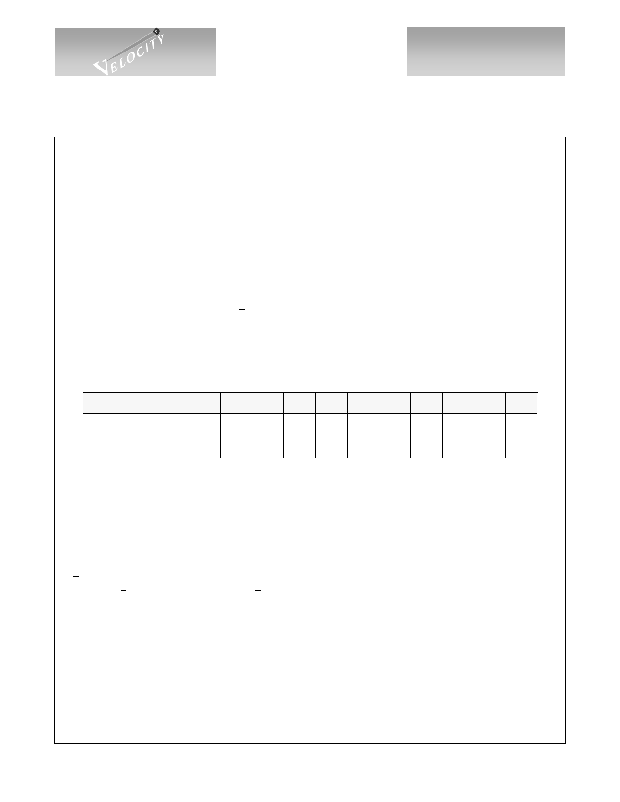
Table 1: Transmission Order and Mapping of a 10B Character
Data Bit
Tx9 Tx8 Tx7 Tx6 Tx5 Tx4 Tx3 Tx2 Tx1 Tx0
10B Bit Position
j
h
g
f
i
e
d
c
b
a
Comma Character
x
x
x
1
1
1
1
1
0
0
Clock Recovery
The VSC7139 accepts differential high speed serial input from the selected source (either the PECL Rx+/
Rx- pins or the internal Tx+/- data), extracts the clock and retimes the data. Equalizers are included in the
receiver to open the data eye and compensate for InterSymbol Interference (ISI) which may be present in the
incoming data. The serial bit stream should be encoded so as to provide DC balance and limited run length by
an 8B/10B encoding scheme. The digital Clock Recovery Unit (CRU) is completely monolithic and requires no
external components. For proper operation, the baud rate of the data stream to be recovered should be within
+200 ppm of ten times the REF frequency. For example, Gigabit Ethernet systems would use 125MHz oscilla-
tors with a +100ppm accuracy resulting in +200 ppm between VSC7139 pairs.
Deserializer
The recovered serial bit stream is converted into a 10-bit parallel output character. The VSC7139 provides
complementary TTL recovered clocks, RCx0 and RCx1, which are at one-twentieth of the serial baud rate (if
RCM=LOW) or one-tenth (if RCM=HIGH). The clocks are generated by dividing down the high-speed recov-
ered clock which is phase locked to the serial data. The serial data is retimed, deserialized and output on
Rx(0:9).
If serial input data is not present, or does not meet the required baud rate, the VSC7139 will continue to
produce a recovered clock so that downstream logic may continue to function. The RCx0/RCx1 output fre-
quency under these circumstances will differ from its expected frequency by no more than +1%.
G52196-0, Rev 3.3
5/14/01
© VITESSE SEMICONDUCTOR CORPORATION • 741 Calle Plano • Camarillo, CA 93012
Tel: (800) VITESSE • FAX: (805) 987-5896 • Email: prodinfo@vitesse.com
Internet: www.vitesse.com
Page 3
Share Link: 