TDA9103 Ver la hoja de datos (PDF) - STMicroelectronics
Número de pieza
componentes Descripción
Fabricante
TDA9103 Datasheet PDF : 27 Pages
| |||
TDA9103
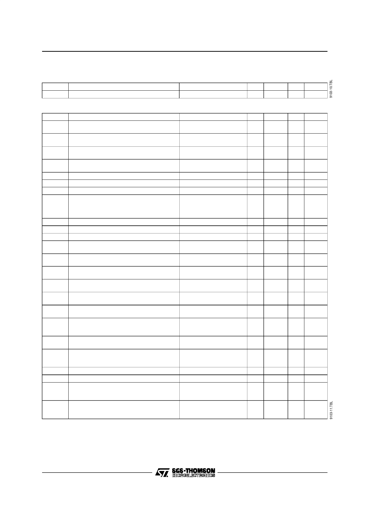
VERTICAL SECTION
Operating Conditions
Symbol
Parameter
VSVR Vertical Sync Input Voltage Range
Test conditions
On Pin 34
Min. Typ. Max. Unit
0
5.5
V
Electrical Characteristics (VCC = 12V, Tamb = 25°C)
Symbol
Parameter
Test conditions
Min. Typ. Max. Unit
IBIASP Pin 23-28-29 Bias Current (Current Sourced For V23-28-29 = 2V
by PNP Base)
2
µA
IBIASN Pin 31 Bias Current (Current Sunk by NPN For V31 = 6V
Base)
0.5
µA
VSth Vertical Sync Input Threshold Voltage
Pin 34; High-level
2
Low-level
V
0.8
V
VSBI Vertical Sync Input Bias Current (Current
Sourced by PNP Base)
V34 = 0.8V
1
µA
VRB Voltage at Ramp Bottom Point
On Pin 27
2/8
VREF-V
VRT
VRTF
Voltage at Ramp Top Point (with Sync)
Voltage at Ramp Top Point (without Sync)
On Pin 27
On Pin 27
5/8
VRT-0.1
VREF-V
V
IR27 Output Current Range on Pin 27 during
Ramp Charging Time. Current to Charge
Capacitor between Pin 27 and Ground
V28 = 2V (Note 2),
2V < V27 < 5V
Min current
Max current
15
20
µA
100 135
µA
VSW Minimum Vertical Sync Pulse Width
Pin 34
5
µS
VSmDut Vertical Sync Input Maximum Duty-cycle
Pin 34
15
%
VSTD Vertical Sawtooth Discharge Time Duration On Pin 27, with 150nF cap
85
µS
VFRF Vertical Free Running Frequency (V28 = 2V) Measured on Pin 27
Cosc (Pin27) = 150nF
100
Hz
ASFR AUTO-SYNC Frequency Range
(see Note 3)
With C27 = 150nF ±5%
50
150 Hz
RATD Ramp Amplitude Thermal Drift
RAFD Ramp Amplitude Drift Versus Frequency
On Pin 30 (see Note 1)
(0°C < Tamb < 70°C)
V31 = 6V, C27 = 150nF
50Hz < F < 120Hz
100
ppm/°C
200
ppm/Hz
Rlin Ramp Linearity on Pin 27 ∆I27/I27
V28 = 2V, V25 = 4.3V
2.5V < V27 < 4.5V
0.5
%
Rload Minimum Load on Pin 25 for less than 1%
Vertical Amplitude Drift
50
MΩ
Vpos
Vertical Position Adjustment Range Voltage V33 = 2V
on Pin 32
V33 = 4V
V33 = 6V
3.2
3.3
V
3.5
V
3.65 3.8
V
IVPOS Max Current on Vertical Position Control
Output (Pin 32)
±2
mA
Vor Vertical Output Voltage Range (on Pin 30)
(Peak to Peak Voltage on Pin 30)
VOUTDC DC Voltage on Vertical Output (Pin30)
V31 = 2V
V31 = 4V
V31 = 6V
See Note 4
2
3
3.75 4
7/16
2.2
V
V
V
VREF-V
V0I Vertical Output Maximum Output Current On Pin 30
±5
mA
dVS Max Vertical S-Correction Amplitude
∆V/V30pp at T/4
(V28 = 2V Inhibits S-CORR; V28 = 6V gives ∆V/V30pp at 3T/4
Maximum S-CORR) (see Figure 3)
-4
%
+4
%
Ccorr
C-Correction Adjustment Range Voltage on
Pin 27 for Maximum Slope on the Ramp
(with S-Correction) (see Figure 4)
V29 = 2V
V29 = 4V
V29 = 6V
3
V
3.5
V
4
V
Notes : 1. These parameters are not tested on each unit. They are measured during our internal qualification procedure which includes
characterization on batches comming from corners of our processes and also temperature characterization.
2. When 2V are applied on Pin 28 (Vertical S-Correction control), then the S-Correction is inhibited, consequently the sawtooth have
a linear shape.
3. It is the frequency range for which the VERTICAL OSCILLATOR will automatically synchronize, using a single capacitor value on
Pin 27 and with a constant ramp amplitude.
4. Typically 3.5V for Vertical reference voltage typical value (8V).
8/27
Share Link: 