VN5012AK-E Ver la hoja de datos (PDF) - STMicroelectronics
Número de pieza
componentes Descripción
Fabricante
VN5012AK-E
STMicroelectronics

VN5012AK-E Datasheet PDF : 30 Pages
| |||
VN5012AK-E
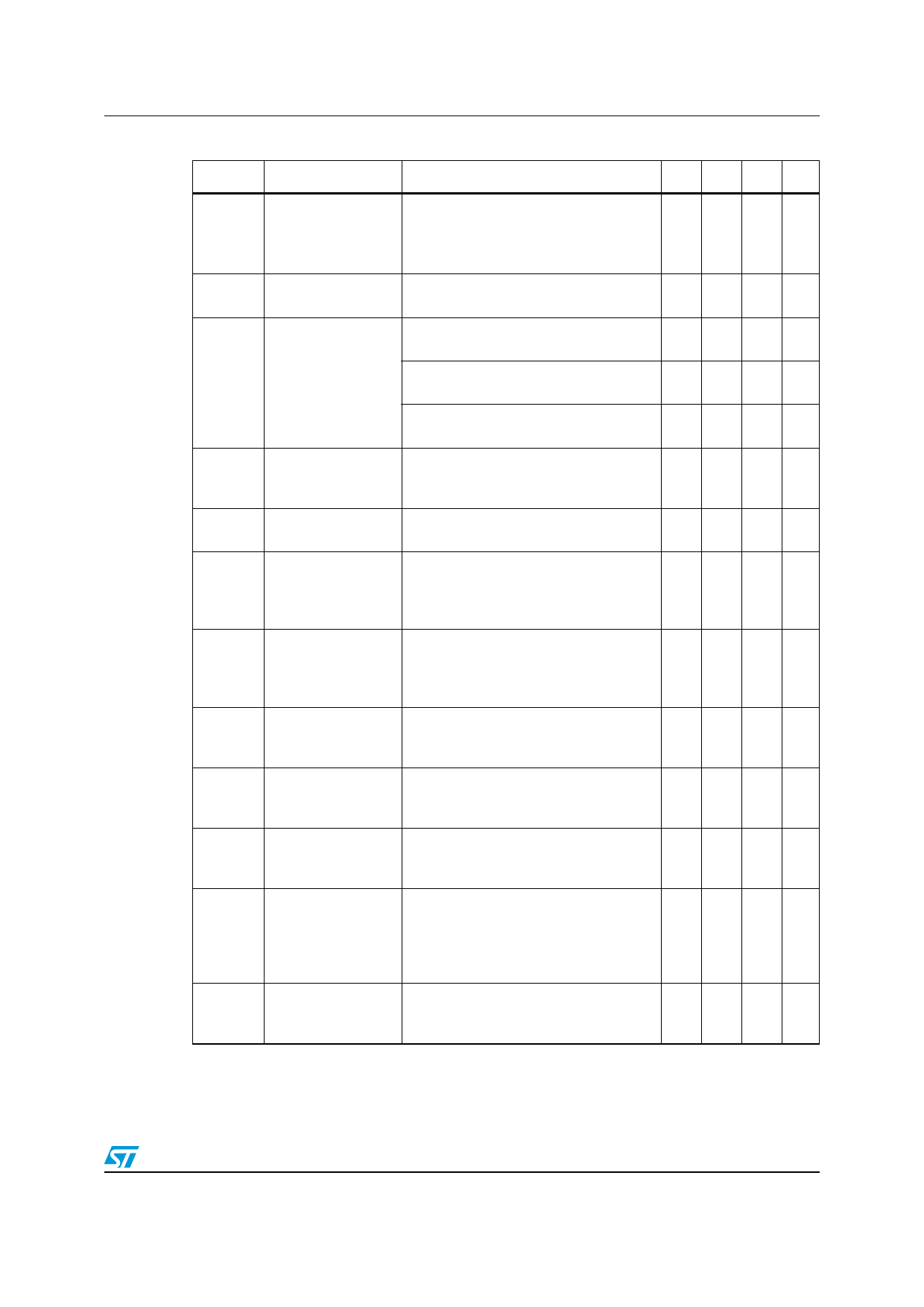
Electrical specifications
Table 10. Current sense (8 V < VCC < 16 V) (continued)
Symbol
Parameter
Test conditions
Min. Typ. Max. Unit
K3
IOUT/ISENSE
dK3/K3(1)
Current sense ratio
drift
ISENSE0
Analog sense
leakage current
Openload on-state
IOL current detection
threshold
IOUT = 25 A; VSENSE = 4 V; VCSD = 0 V;
Tj = -40 °C to 150 °C
IOUT = 25 A; VSENSE = 4 V; VCSD = 0 V;
Tj = 25 °C to 150 °C
4420 4600 4780
4460 4600 4740
IOUT = 25 A; VSENSE = 4 V; VCSD = 0 V;
Tj = -40 °C to 150 °C
-4
+4 %
IOUT = 0 A; VSENSE = 0 V; VCSD = 5 V;
VIN = 0 V; Tj = -40 °C to 150 °C
0
1 µA
IOUT = 0 A; VSENSE = 0 V; VCSD = 0 V;
VIN = 5 V; Tj = -40 °C to 150 °C
0
2 µA
IOUT = 2 A; VSENSE = 0 V; VCSD = 5 V;
VIN = 5 V; Tj = -40 °C to 150 °C
0
1 µA
VIN = 5 V; ISENSE = 5 µA
10
45 mA
VSENSE
Max analog sense
output voltage
IOUT = 15 A; VCSD = 0 V
5
V
VSENSEH
Analog sense output
voltage in over
temperature
condition
VCC = 13 V; RSENSE = 2.2 KΩ
9
V
ISENSEH
Analog sense output
current in over
temperature
condition
VCC = 13 V; VSENSE = 5 V
8
mA
Delay response time VSENSE < 4 V; 1.5 A < IOUT < 25 A;
tDSENSE1H from falling edge of ISENSE = 90 % of ISENSE max
CS_DIS pin
(see Figure 4)
50 100 µs
Delay response time VSENSE < 4 V; 1.5 A < IOUT < 25 A;
tDSENSE1L from rising edge of ISENSE = 10 % of ISENSE max
CS_DIS pin
(see Figure 4)
5 20 µs
Delay response time VSENSE < 4 V; 1.5 A < IOUT < 25 A;
tDSENSE2H from rising edge of ISENSE = 90 % of ISENSE max
INPUT pin
(see Figure 4)
270 400 µs
ΔtDSENSE2H
Delay response time
between rising edge
of output current and
rising edge of
current sense
VSENSE < 4 V;
ISENSE = 90 % of ISENSEMAX;
IOUT = 90 % of IOUTMAX;
IOUTMAX = 5 A (see Figure 5)
300 µs
Delay response time VSENSE < 4 V; 1.5 A < IOUT < 25 A;
tDSENSE2L from falling edge of ISENSE = 10 % of ISENSE max
INPUT pin
(see Figure 4)
100 250 µs
1. Parameter guaranteed by design, it is not tested.
Doc ID 13240 Rev 9
11/30
Share Link: