VN5050JTR-E Ver la hoja de datos (PDF) - STMicroelectronics
Número de pieza
componentes Descripción
Fabricante
VN5050JTR-E Datasheet PDF : 31 Pages
| |||
Application information
3
Application information
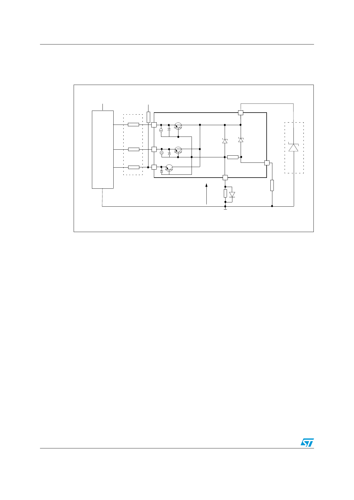
Figure 27. Application schematic
+5V
+5V
VCC
Rprot
STAT_DIS
Rprot
C
Rprot
INPUT
STATUS
GND
VGND
RGND
OUTPUT
DGND
VN5050J-E
Dld
3.1
3.1.1
20/31
GND protection network against reverse battery
Solution 1: resistor in the ground line (RGND only)
This can be used with any type of load.
The following is an indication on how to dimension the RGND resistor.
1. RGND 600mV / (IS(on)max).
2. RGND VCC) / (-IGND)
where -IGND is the DC reverse ground pin current and can be found in the absolute
maximum rating section of the device datasheet.
Power Dissipation in RGND (when VCC<0: during reverse battery situations) is:
PD= (-VCC)2/RGND
This resistor can be shared amongst several different HSDs. Please note that the value of
this resistor should be calculated with formula (1) where IS(on)max becomes the sum of the
maximum on-state currents of the different devices.
Please note that if the microprocessor ground is not shared by the device ground then the
RGND will produce a shift (IS(on)max * RGND) in the input thresholds and the status output
values. This shift will vary depending on how many devices are ON in the case of several
high side drivers sharing the same RGND.
If the calculated power dissipation leads to a large resistor or several devices have to share
the same resistor then ST suggests to utilize Solution 2 (see below).
Share Link: 