UPSD3233 Ver la hoja de datos (PDF) - STMicroelectronics
Número de pieza
componentes Descripción
Fabricante
UPSD3233
STMicroelectronics

UPSD3233 Datasheet PDF : 170 Pages
| |||
uPSD3234A, uPSD3234BV, uPSD3233B, uPSD3233BV
ARCHITECTURE OVERVIEW
Memory Organization
The uPSD323X Devices’s standard 8032 Core
has separate 64KB address spaces for Program
memory and Data Memory. Program memory is
where the 8032 executes instructions from. Data
memory is used to hold data variables. Flash
memory can be mapped in either program or data
space. The Flash memory consists of two flash
memory blocks: the main Flash (1 or 2Mbit) and
the Secondary Flash (256Kbit). Except during
flash memory programming or update, Flash
memory can only be read, not written to. A Page
Register is used to access memory beyond the
64K bytes address space. Refer to the PSD Mod-
ule for details on mapping of the Flash memory.
The 8032 core has two types of data memory (in-
ternal and external) that can be read and written.
The internal SRAM consists of 256 bytes, and in-
cludes the stack area.
The SFR (Special Function Registers) occupies
the upper 128 bytes of the internal SRAM, the reg-
isters can be accessed by Direct addressing only.
There are two separate blocks of external SRAM
inside the uPSD323X Devices: one 256 bytes
block is assigned for DDC data storage. Another
8K bytes resides in the PSD Module that can be
mapped to any address space defined by the user.
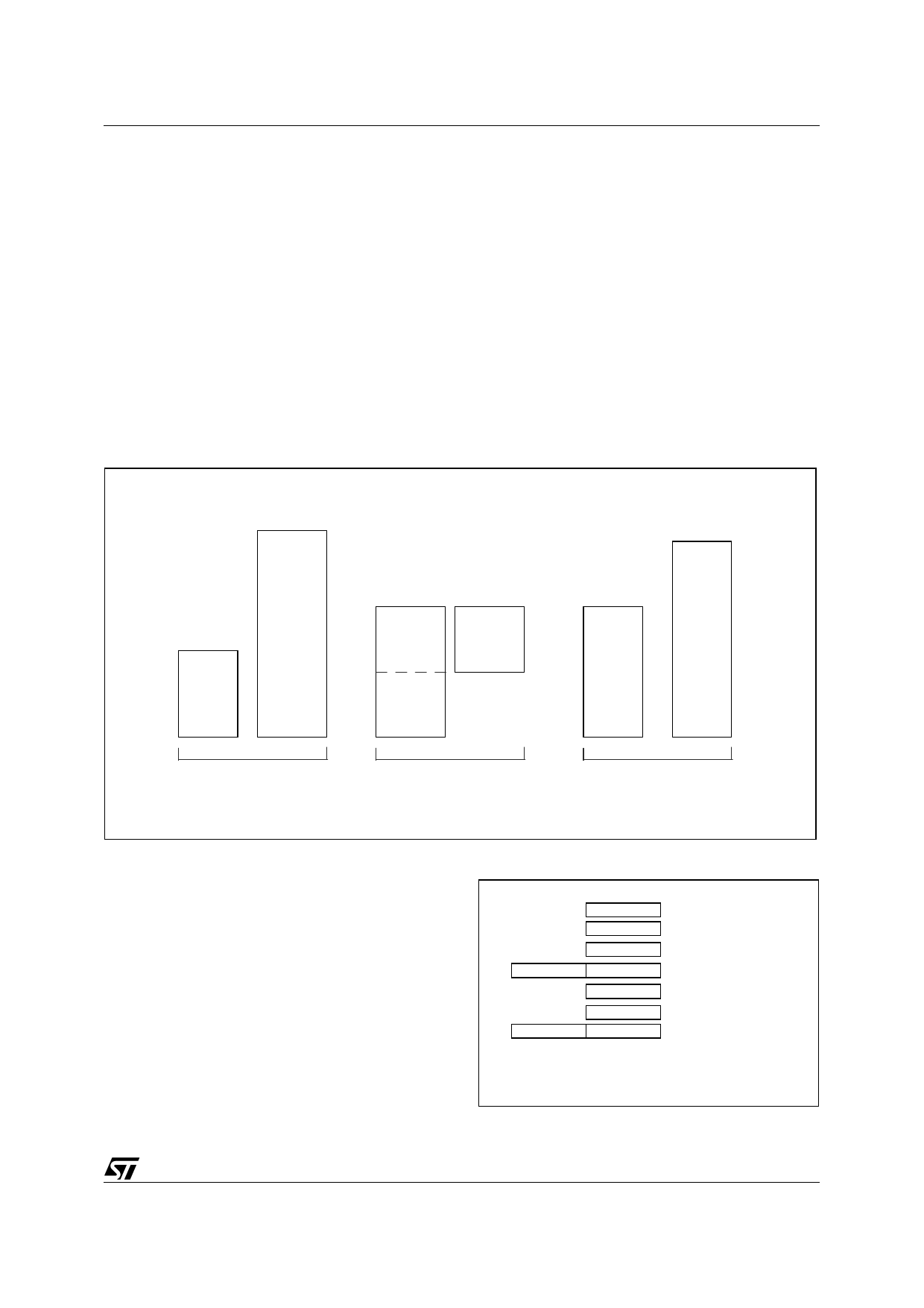
Figure 5. Memory Map and Address Space
MAIN
FLASH
EXT. RAM
INT. RAM SFR
EXT. RAM
(DDC)
FF
FFFF
SECONDARY
FLASH
Indirect
Direct
128KB
Addressing Addressing
256B
8KB
32KB
OR
256KB
7F
Indirect
or
Direct
Addressing
0
FF00
Flash Memory Space
Internal RAM Space
(256 Bytes)
External RAM Space
(MOVX)
AI06635
Registers
The 8032 has several registers; these are the Pro-
gram Counter (PC), Accumulator (A), B Register
(B), the Stack Pointer (SP), the Program Status
Word (PSW), General purpose registers (R0 to
R7), and DPTR (Data Pointer register).
Figure 6. 8032 MCU Registers
PCH
DPTR(DPH)
A
B
SP
PCL
PSW
R0-R7
DPTR(DPL)
Accumulator
B Register
Stack Pointer
Program Counter
Program Status Word
General Purpose
Register (Bank0-3)
Data Pointer Register
AI06636
13/170
Share Link: