UPD63335 Ver la hoja de datos (PDF) - NEC => Renesas Technology
Número de pieza
componentes Descripción
Fabricante
UPD63335 Datasheet PDF : 56 Pages
| |||
µ PD63335
1. DESCRIPTION OF FUNCTIONS
1.1 Analog Input Block
The µPD63335 features an on-chip two-channel ADC, which can convert analog signals selected by the
multiplexer at the previous stage and input via the analog input pin to digital signals. An amplifier is configured
between the ADC and multiplexer, and the input gain can be set in a range from 0 dB to 22.5 dB.
The multiplexer receives signals that are input from the analog output block’s mixer circuit, and four-channel
stereo signals, two monaural signals, and a monaural MIC input signal (selected from two input pins) from the analog
input pins.
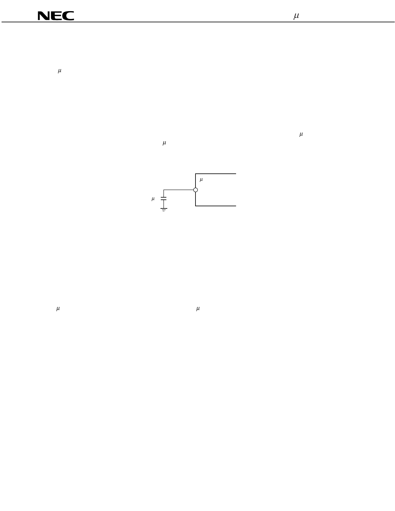
The IN1 input has a dedicated AC ground pin for canceling common-mode noise. Use of the IN1_GND pin
enables connections to output pins that have a ground line, such as a CD audio output pin, via a 4.7 µF capacitor. If
not using IN1_GND, connect to a ground via a 1 µF capacitor (see Figure 1-1).
Figure 1-1. Connection Example When Not Using IN1_GND
1 µF
µPD63335
IN1_GND
1.2 Analog Output Block
The analog output block includes two stereo output amplifiers, a monaural output amplifier, and a mixer circuit.
The mixer circuit can be used to mix not only stereo analog signals from the DAC but also four pairs of stereo signals
(IN1 to IN4), one monaural signal, and one MIC input signal (selected from two input pins). The analog signals from
the DAC output can be connected to the mixer circuit or DAC L/R output via volume circuits. Monaural mixed signals
to the monaural output selector (MIX) are the sum of the L channel/R channel mixer circuit output to which –6 dB of
gain adjustment is applied within the LSI.
1.3 Clock
The µPD63335 features an on-chip clock generator. The µPD63335’s master clock can be generated if a crystal
resonator is connected via the XTL_IN or XTL_OUT pin.
The on-chip clock generator can be used only at the 24.576 MHz setting.
In addition, an external master clock can be input to the on-chip clock generator. In such cases, input the clock
signal directly to the XTL_IN pin and leave the XTL_OUT pin open. In this case, the recommended frequency range
of the external master clock is from 1.024 MHz to 24.576 MHz.
8
Data Sheet S15003EJ6V0DS
Share Link: 