UPD4712C Ver la hoja de datos (PDF) - NEC => Renesas Technology
Número de pieza
componentes Descripción
Fabricante
UPD4712C Datasheet PDF : 12 Pages
| |||
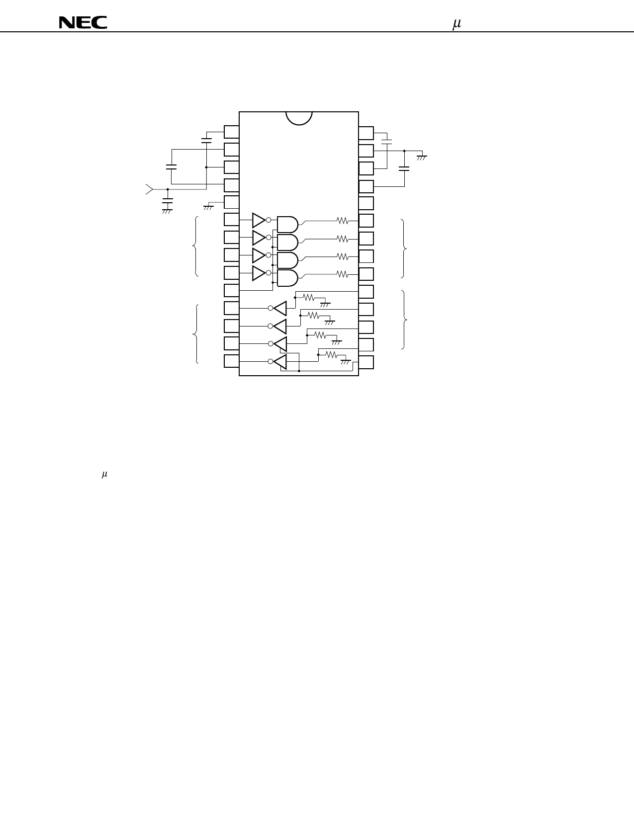
BLOCK DIAGRAM/PIN CONFIGURATION (Top View)
µPD4712C/4712D
+
C1
+5 V
+10 V
+
C3
Bypass
capasitor
DIN1
TTL/CMOS DIN2
INPUT
DIN3
1 VDD
2 C1+
3 VCC
4 C1–
5 GND
6
7
8
DIN4 9
Output control DCON 10
ROUT1 11
TTL/CMOS
OUTPUT
ROUT2 12
ROUT3 13
ROUT4 14
DC-DC
converter
C4+ 28
GND 27
C4– 26
+
C4
+
C2
VSS 25
–10 V
24 STBY Standby
5.5 kΩ
300 Ω
300 Ω
300 Ω
300 Ω
23 DOUT1
22 DOUT2
21 DOUT3
20 DOUT4
19 RIN1
18 RIN2
5.5 kΩ
17 RIN3
RS-232
OUTPUT
RS-232
INPUT
5.5 kΩ
16 RIN4
5.5 kΩ
15 RCON
Threshold control
* VDD and Vss are output pins of voltages internally boosted. Connecting a load directly to these pins is not
recommended.
** The standby pin is internally pulled down.
*** Use capacitors with a working voltage of 16 V or higher as C1 through C4. Insert a bypass capasitor about 0.1
to 1 µF between VCC pin to GND pin.
2
Share Link: 