UPD16312GB-3B4 Ver la hoja de datos (PDF) - NEC => Renesas Technology
Número de pieza
componentes Descripción
Fabricante
UPD16312GB-3B4 Datasheet PDF : 20 Pages
| |||
PD16312
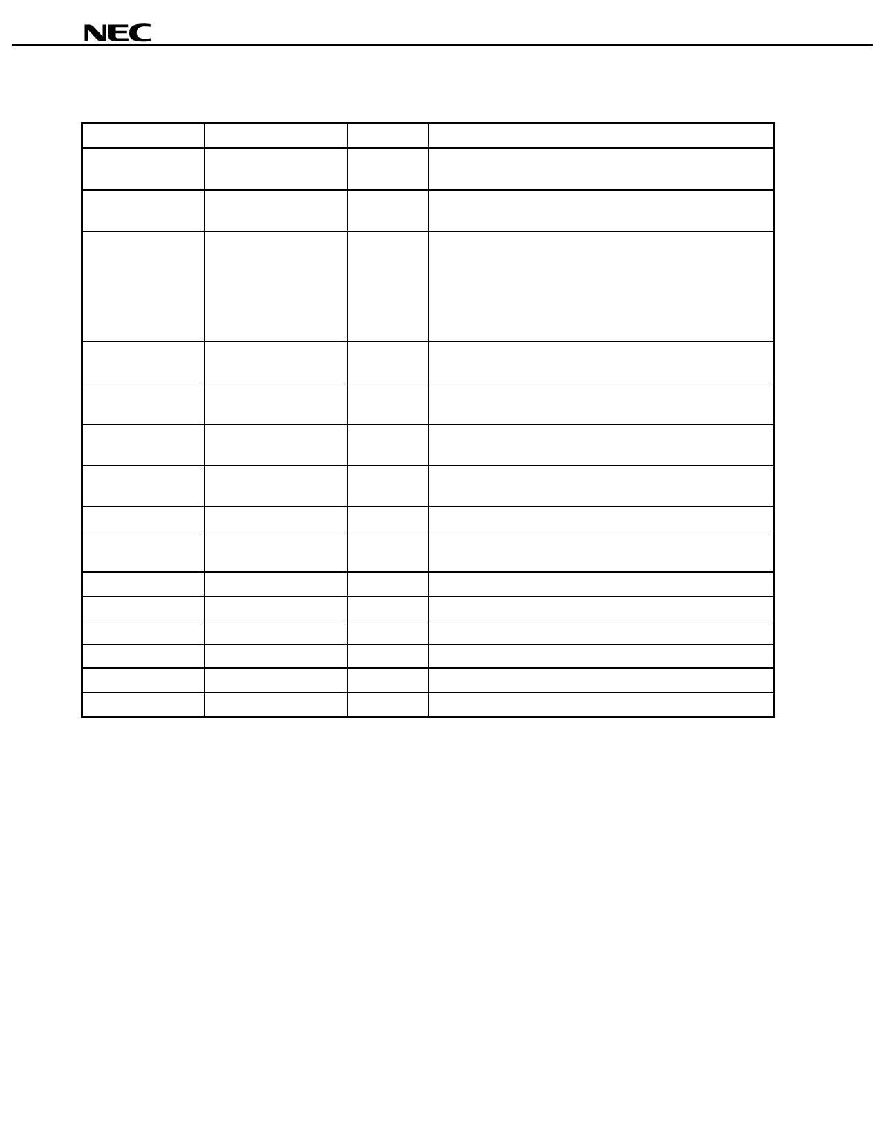
Pin Function
Symbol
DIN
DOUT
STB
CLK
OSC
Seg1/KS1 to
Seg6/KS6
Seg7 to Seg11
Grid1 to Grid6
Seg12/Grid11 to
Seg16/Grid7
LED1 to LED4
KEY1 to KEY4
SW1 to SW4
VDD
VSS
VEE
Pin Name
Data input
Data output
Strobe
Clock input
Oscillator pin
High-voltage output
Pin No
6
5
9
8
44
15 to 20
Description
Input serial data at rising edge of shift clock, starting from the low
order bit.
Output serial data at the falling edge of the shift clock, starting
from low order bit. This is N-ch open-drain output pin.
Initializes serial interface at the rising or falling edge of the
PD16312. It then waits for reception of a command. Data input
after STB has fallen is processed as a command. While
command data is processed, current processing is stopped, and
the serial interface is initialized. While STB is high, CLK is
ignored.
Reads serial data at the rising edge, and outputs data at the
falling edge.
Connect resistor to this pin to determine the oscillation frequency
to this pin.
Segment output pins (Dual function as key source)
High-voltage output
(segment)
High-voltage output (grid)
High-voltage output
(segment/grid)
LED output
Key data input
Switch input
Logic power
Logic ground
Pull-down level
21 to 25 Segment output pins
37 to 32 Grid output pins
26, 28 to 31 These pins are selectable for segment or grid driving.
42 to 39
10 to 13
1 to 4
14, 38
7, 43
27
CMOS output. +20 mA max.
Data input to these pins is latched at the end of the display cycle.
These pins constitute a 4-bit general-purpose input port.
5 V 10 %
Connect this pin to system GND.
VDD 35 V max.
4
Share Link: 