UPD12115 Ver la hoja de datos (PDF) - NEC => Renesas Technology
Número de pieza
componentes Descripción
Fabricante
UPD12115 Datasheet PDF : 10 Pages
| |||
μ PD12115
CIN : 0.1 μ F or higher. Be sure to connect CIN to prevent parasitic oscillation. Set this value according to the length
of the line between the regulator and the INPUT pin. Use of a film capacitor or other capacitor with first-rate
voltage and temperature characteristics is recommended. If using a laminated ceramic capacitor, it is necessary
to ensure that CIN is 0.1 μ F or higher for the voltage and temperature range to be used.
COUT: 10 μ F or higher. Be sure to connect COUT to prevent oscillation and improve excessive load regulation. Place
CIN and COUT as close as possible to the IC pins (within 1 to 2 cm). Also, in case of using a laminated ceramic
capacitor, please note following items.
• It is necessary to ensure that COUT is 10 μ F or higher for the voltage and temperature range to be used.
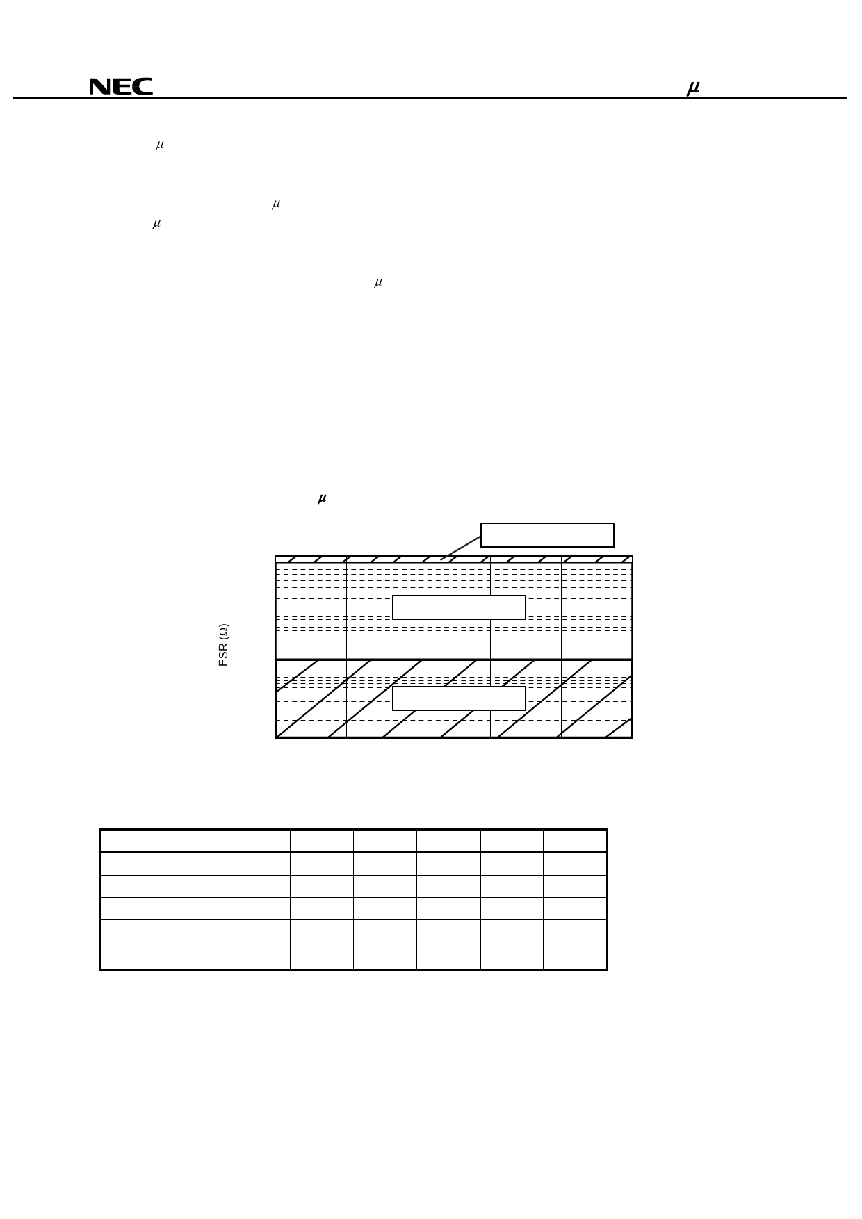
• In case of using laminated ceramic capacitor, it is easy to become state of parasitic oscillation. Because ESR
of laminated ceramic capacitor is very low. Therefore, the capacitor and load condition (output current) which
fulfill the condition of the stable operation area of ESR shown below are recommended.
• Stable Operation Area as below is regulated under condition of which this product is not on a substrate.
Therefore impedance on substrate is not considered.
D1 : If the OUTPUT pin has a higher voltage than the INPUT pin, connect a diode.
D2 : If the OUTPUT pin has a lower voltage than the GND pin, connect a Schottky barrier diode.
Caution Make sure that no external voltage is applied to the OUTPUT pin.
μ PD12115 COUT ESR Stable Operation Area
Unstable Operation Area
10
1
Stable Operation Area
0.1
Unstable Operation Area
0.01
0
200
400
600
800
1000
IO (mA)
RECOMMENDED OPERATING CONDITIONS
Parameter
Symbol
MIN.
TYP.
MAX.
Unit
Input Voltage
VIN
2.5
ON/OFF Pin Voltage
VON/OFF
0
Output Current
IO
0
Operating Ambient Temperature
TA
− 40
5.5
V
VIN
V
1.0
A
+ 85
°C
Operating Junction Temperature
TJ
− 40
+ 125
°C
Caution1. Turn on VIN and VON/OFF at the same time, or turn on VIN first and then VON/OFF.
Turn off VIN and VON/OFF at the same time, or turn off VON/OFF first and then VIN.
2. If absolute maximum rating is not exceeded, you can used this product above the recommended
operating range. However, since a margin with absolute maximum rating decreases, please use
this product after sufficient evaluation.
Data Sheet G18851EJ1V0DS
3
Share Link: 