UPD160062 Ver la hoja de datos (PDF) - NEC => Renesas Technology
Número de pieza
componentes Descripción
Fabricante
UPD160062 Datasheet PDF : 18 Pages
| |||
µ PD160062
5. RELATIONSHIP BETWEEN INPUT DATA AND OUTPUT VOLTAGE VALUE
The µ PD160062 incorporates a 6-bit D/A converter whose odd output pins and even output pins output respectively
gray scale voltages of differing polarity with respect to the LCD’s counter electrode (common electrode) voltage. The
D/A converter consists of ladder resistors and switches.
The ladder resistors (r0 to r62) are designed so that the ratio of LCD panel γ -compensated voltages to V0’ to V63’
and V0” to V63” is almost equivalent. For the 2 sets of five γ -compensated power supplies, V0 to V4 and V5 to V9,
respectively, input gray scale voltages of the same polarity with respect to the common voltage. When fine gray scale
voltage precision is not necessary, there is no need to connect a voltage follower circuit to the γ -compensated power
supplies V1 to V3 and V6 to V8.
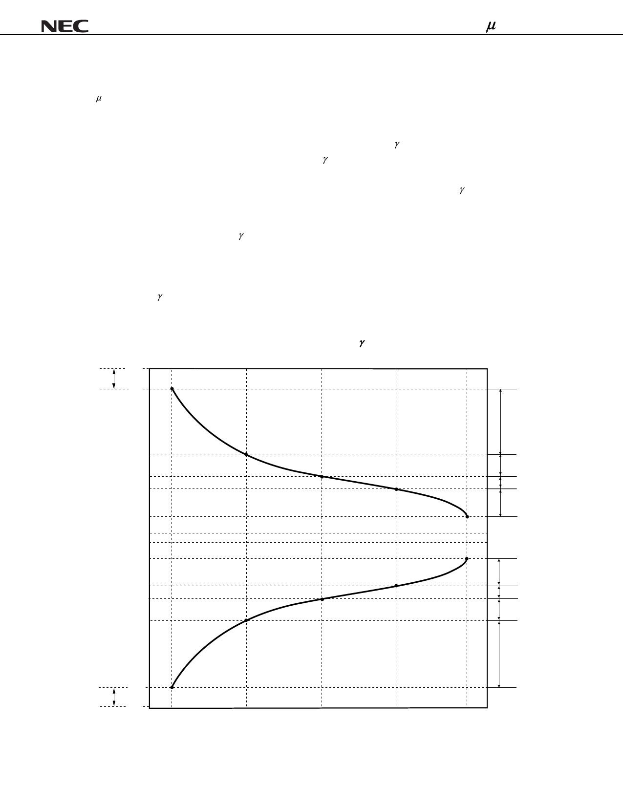
Figure 5−1 shows the relationship between the driving voltages such as liquid-crystal driving voltages VDD2 and VSS2,
common electrode potential VCOM, and γ -corrected voltages V0 to V9 and the input data. Be sure to maintain the
voltage relationships of
VDD2 −0.1 V ≥ V0 > V1 > V2 > V3 > V4 ≥ 0.5 VDD2
0.5 VDD2 ≥ V5 > V6 > V7 > V8 > V9 ≥ VSS2 +0.1 V
Figures 5−2 shows γ -corrected power supply voltage and ladder resistors ratio and figure 5−3 shows the relationship
between the input data and the output voltage.
Figure 5−1. Relationship between Input Data and γ -corrected Power Supplies
0.1 V
VDD2
V0
Split interval
16
V1
16
V2
16
V3
15
V4
VCOM
0.5 VDD2
V5
15
V6
16
V7
16
V8
16
V9
0.1 V
VSS2
00
10
20
30
3F
Input data (HEX)
6
Data Sheet S16449EJ1V0DS
Share Link: 