UPD160062 Ver la hoja de datos (PDF) - NEC => Renesas Technology
Número de pieza
componentes Descripción
Fabricante
UPD160062 Datasheet PDF : 18 Pages
| |||
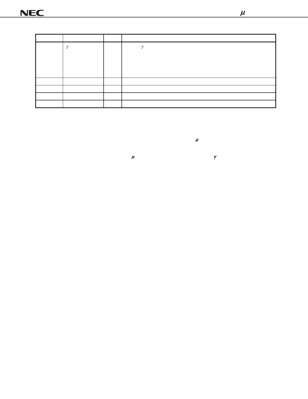
µ PD160062
Pin Symbol
Pin Name
I/O
V0 to V9
γ -corrected power
−
supplies
VDD1
VDD2
VSS1
VSS2
Logic power supply
−
Driver power supply −
Logic ground
−
Driver ground
−
(2/2)
Description
Input the γ -corrected power supplies from outside by using operational amplifier.
Make sure to maintain the following relationships. During the gray scale voltage
output, be sure to keep the gray scale level power supply at a constant level.
VDD2 −0.1 V ≥ V0 > V1 > V2 > V3 > V4 ≥ 0.5 V DD2
0.5 V DD2 ≥ V5 > V6 > V7 > V8 > V9 ≥ VSS2 +0.1 V
2.3 to 3.6 V
8.0 to 9.0 V
Grounding
Grounding
Cautions 1. The power start sequence must be VDD1, logic input, and VDD2 & V0 to V9 in that order. Reverse
this sequence to shut down.
2. To stabilize the supply voltage, please be sure to insert a 0.1 µF bypass capacitor between
VDD1-VSS1 and VDD2-VSS2. Furthermore, for increased precision of the D/A converter, insertion of a
bypass capacitor of about 0.01 µF is also recommended between the γ -corrected power supply
terminals (V0, V1, V2, ···, V9) and VSS2.
Data Sheet S16449EJ1V0DS
5
Share Link: 