UPD160061ANL-XXX Ver la hoja de datos (PDF) - NEC => Renesas Technology
Número de pieza
componentes Descripción
Fabricante
UPD160061ANL-XXX
NEC => Renesas Technology

UPD160061ANL-XXX Datasheet PDF : 18 Pages
| |||
µPD160061A
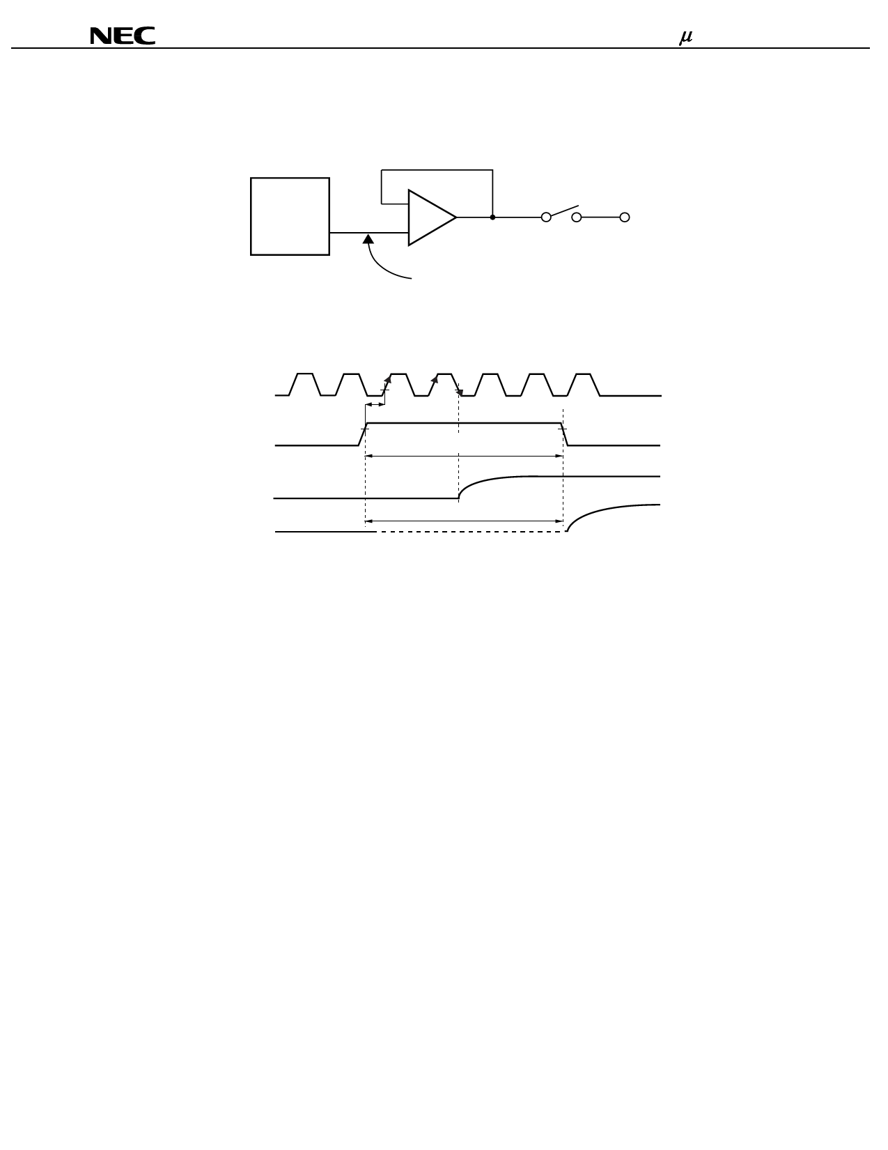
7. RELATIONSHIP BETWEEN STB CLK AND OUTPUT WAVEFORM
Figure 7–1. Input Circuit Block Diagram
DAC
Output AMP.
-
+
VAMP(IN)
SW1
Sn
(VX)
CLK
STB
VAMP(IN)
Sn(VX)
Figure 7–2. Output Circuit Timing Waveform
[1] [1']
tSTB-CLK
SW1: OFF
Hi-Z
STB = H is loaded with the rising edge of CLK[1]. However, when not satisfying the specification of fSTB-CLK, STB = H is
loaded with the rising edge of the next CLK[1′]. Latch operation of display data is completed with the falling edge of the
next CLK which loaded STB = H. Therefore, in order to complete latch operation of display data, it is necessary to input
at least 2 CLK in STB = H period. Besides, after loading STB=H to the timing of [1], it is necessary to continue inputting
CLK.
10
Data Sheet S16041EJ2V0DS
Share Link: