UPD160040B Ver la hoja de datos (PDF) - NEC => Renesas Technology
Número de pieza
componentes Descripción
Fabricante
UPD160040B
NEC => Renesas Technology

UPD160040B Datasheet PDF : 19 Pages
| |||
µPD160040B
5. RELATIONSHIP BETWEEN INPUT DATA AND OUTPUT VOLTAGE VALUE
The µPD160040B incorporates a 8-bit D/A converter whose odd output pins and even output pins output
respectively gray scale voltages of differing polarity with respect to the LCD’s counter electrode voltage. The D/A
converter consists of ladder resistors and switches.
The ladder resistors (r0 to r254) are designed so that the ratio of LCD panel (γ -compensated voltages to V0’-V255’ and
V0”-V255” is almost equivalent as shown in Figure 5−2. For the 2 sets of eight γ -compensated power supplies, V0-V7
and V8-V15, respectively, input gray scale voltages of the same polarity with respect to the 0.5 VDD2.
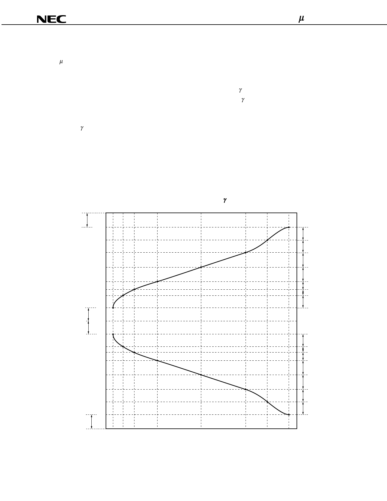
Figure 5−1 shows the relationship between the driving voltages such as liquid-crystal driving voltages VDD2, VSS2 and
0.5 VDD2, and γ -corrected voltages V0-V15 and the input data. Be sure to maintain the voltage relationships below.
VDD2 – 0.2 V ≥ V0 > V1 > V2 > V3 > V4 > V5 > V6 > V7 ≥ 0.5 VDD2 + 0.5 V
0.5 VDD2 – 0.5 V ≥ V8 > V9 > V10 > V11 > V12 > V13 > V14 > V15 ≥ 0.5 VSS2 + 0.2 V
Figures 5−2 and 5−3 show the relation ship between the input data and the output voltage and the resistance values
of the resistor strings.
5
Figure 5−1. Relationship between Input Data and γ -corrected Power Supplies
0.2 V
VDD2
V0
V1
V2
V3
V4
V5
V6
V7
0.5 V
0.5 VDD2
0.5 V
V8
V9
V10
V11
V12
V13
V14
V15
0.2 V
VSS2
00 0F 1F
3F
7F
Input Data (HEX)
32
32
64
64
32
16
15
15
16
32
64
64
32
32
BF
DF
FF
6
Data Sheet S15953EJ2V0DS
Share Link: