UPC8179TB-E3 Ver la hoja de datos (PDF) - NEC => Renesas Technology
Número de pieza
componentes Descripción
Fabricante
UPC8179TB-E3 Datasheet PDF : 28 Pages
| |||
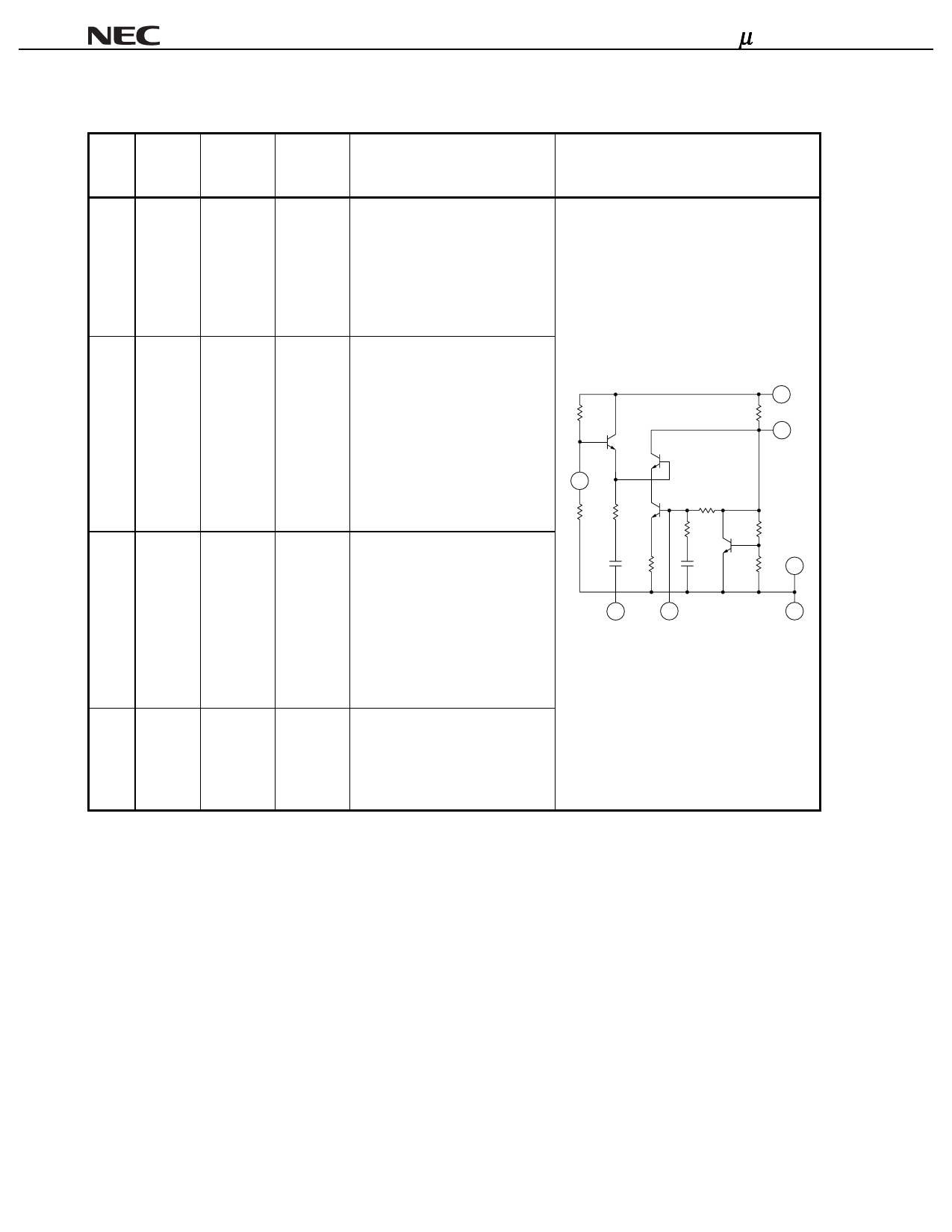
µPC8179TB
PIN EXPLANATION
Pin Pin
Applied
No.
Name
Voltage
(V)
1
INPUT
−
Pin
Voltage
(V)Note
1.09
Function and Applications
Signal input pin. A internal
matching circuit, configured with
resisters, enables 50 Ω connec-
tion over a wide band. This pin
must be coupled to signal source
with capacitor for DC cut.
Internal Equivalent Circuit
2
GND
0
−
Ground pin. This pin should be
3
connected to system ground with
5
minimum inductance. Ground
6
pattern on the board should be
formed as wide as possible.
4
All the ground pins must be con-
nected together with wide ground
pattern to decrease impedance
↓
defference.
4 OUTPUT voltage
−
Signal output pin. This pin is de-
as same
signed as collector output. Due
2
as VCC
to the high impedance output,
through
this pin should be externally
3
1
5
external
equipped with LC matching
inductor
circuit to next stage. For L, a
size 1005 chip inductor can be
chosen.
6
VCC
2.4 to 3.3
−
Power supply pin. This pin
should be externally equipped
with bypass capacitor to
minimize its impedance.
Note Pin voltage is measured at VCC = 3.0 V.
4
Data Sheet P14730EJ2V0DS00
Share Link: 