UPB1008K Ver la hoja de datos (PDF) - NEC => Renesas Technology
Número de pieza
componentes Descripción
Fabricante
UPB1008K Datasheet PDF : 25 Pages
| |||
µPB1008K
Pin
Pin Name
No.
Function and Application
10
REFin
Input pin of reference frequency
buffer. This pin should be
equipped with external 27 MHz
oscillator (e.g. TCXO).
11
GNDdig
Ground pin of digital portion of
the chip.
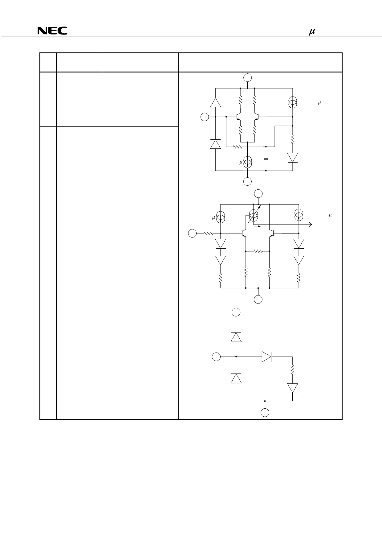
Internal Equivalent Circuit
9
ESD
10
ESD
20 kΩ
500 Ω
50 kΩ
idc = 22 µ
20 kΩ
500 Ω
5.4 pF
idc = 9.7µ
30 kΩ
12
IQ cntl
The voltage on this pin controls
the Q channel IF amplifier gain
control of ±2 dB can be
achieved for 0 to 3 V.
idc = 23.5 µ
Leave open-circuited if not
used.
200 kΩ
12
11
28
IREF
12 kΩ
idc = 23.5 µ
CCCS
13
PD1
Standby mode control.
Low = whole chip OFF & High =
Whole chip ON.
7.1 kΩ
7.1 kΩ
7.1 kΩ
32
VCC
7.1 kΩ
ESD
13
ESD
28 kΩ
11
Data Sheet PU10282EJ01V0DS
5
Share Link: 