UPA1850 Ver la hoja de datos (PDF) - NEC => Renesas Technology
Número de pieza
componentes Descripción
Fabricante
UPA1850 Datasheet PDF : 8 Pages
| |||
µ PA1850
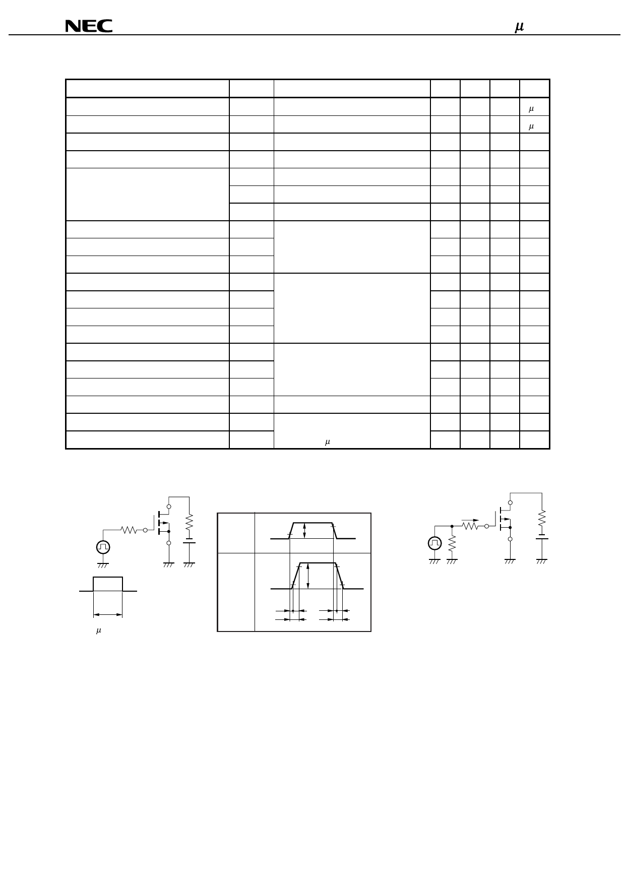
ELECTRICAL CHARACTERISTICS (TA = 25 °C)
CHARACTERISTICS
SYMBOL
TEST CONDITIONS
Drain Cut-off Current
IDSS
VDS = –12 V, VGS = 0 V
Gate Leakage Current
5 Gate to Source Cut-off Voltage
5 Forward Transfer Admittance
IGSS
VGS(off)
| yfs |
VGS = # 10 V, VDS = 0 V
VDS = –10 V, ID = –1 mA
VDS = –10 V, ID = –1.5 A
Drain to Source On-state Resistance
RDS(on)1 VGS = –4.5 V, ID = –1.5 A
RDS(on)2 VGS = –4.0 V, ID = –1.5 A
RDS(on)3 VGS = –2.5 V, ID = –1.5 A
Input Capacitance
Ciss
VDS = –10 V
Output Capacitance
Coss
VGS = 0 V
Reverse Transfer Capacitance
Crss
f = 1 MHz
Turn-on Delay Time
td(on)
VDD = –10 V
Rise Time
tr
ID = –1.5 A
Turn-off Delay Time
td(off)
VGS(on) = –4.0 V
Fall Time
tf
RG = 10 Ω
Total Gate Charge
QG
VDD = –10 V
Gate to Source Charge
QGS ID = –2.5 A
Gate to Drain Charge
QGD VGS = –4.0 V
Diode Forward Voltage
5 Reverse Recovery Time
5 Reverse Recovery Charge
VF(S-D)
trr
Qrr
IF = 2.5 A, VGS = 0 V
IF = 2.5 A, VGS = 0 V
di/dt = 10 A / µs
MIN. TYP. MAX. UNIT
–10 µA
# 10 µA
–0.5 –1.0 –1.5 V
2.0 5.0
S
80 115 mΩ
85 130 mΩ
127 200 mΩ
260
pF
300
pF
45
pF
120
ns
420
ns
520
ns
430
ns
12
nC
2
nC
5
nC
0.80
V
750
ns
950
nC
TEST CIRCUIT 1 SWITCHING TIME
TEST CIRCUIT 2 GATE CHARGE
D.U.T.
RG
PG.
VGS (−)
0
τ
τ = 1µs
Duty Cycle ≤ 1 %
RL
VGS (−)
VGS
Wave Form
10 %
0
VGS(on) 90 %
VDD
ID (−)
90 %
ID
ID
0 10 %
Wave Form
90 %
10 %
td(on) tr td(off) tf
ton
toff
D.U.T.
IG = −2 mA
RL
PG.
50 Ω
VDD
2
Data Sheet D11818EJ2V0DS00
Share Link: 