MX828DS Ver la hoja de datos (PDF) - MX-COM Inc
Número de pieza
componentes Descripción
Fabricante
MX828DS Datasheet PDF : 34 Pages
| |||
CTCSS/DCS/SelCall Processor
4
MX828 PRELIMINARY INFORMATION
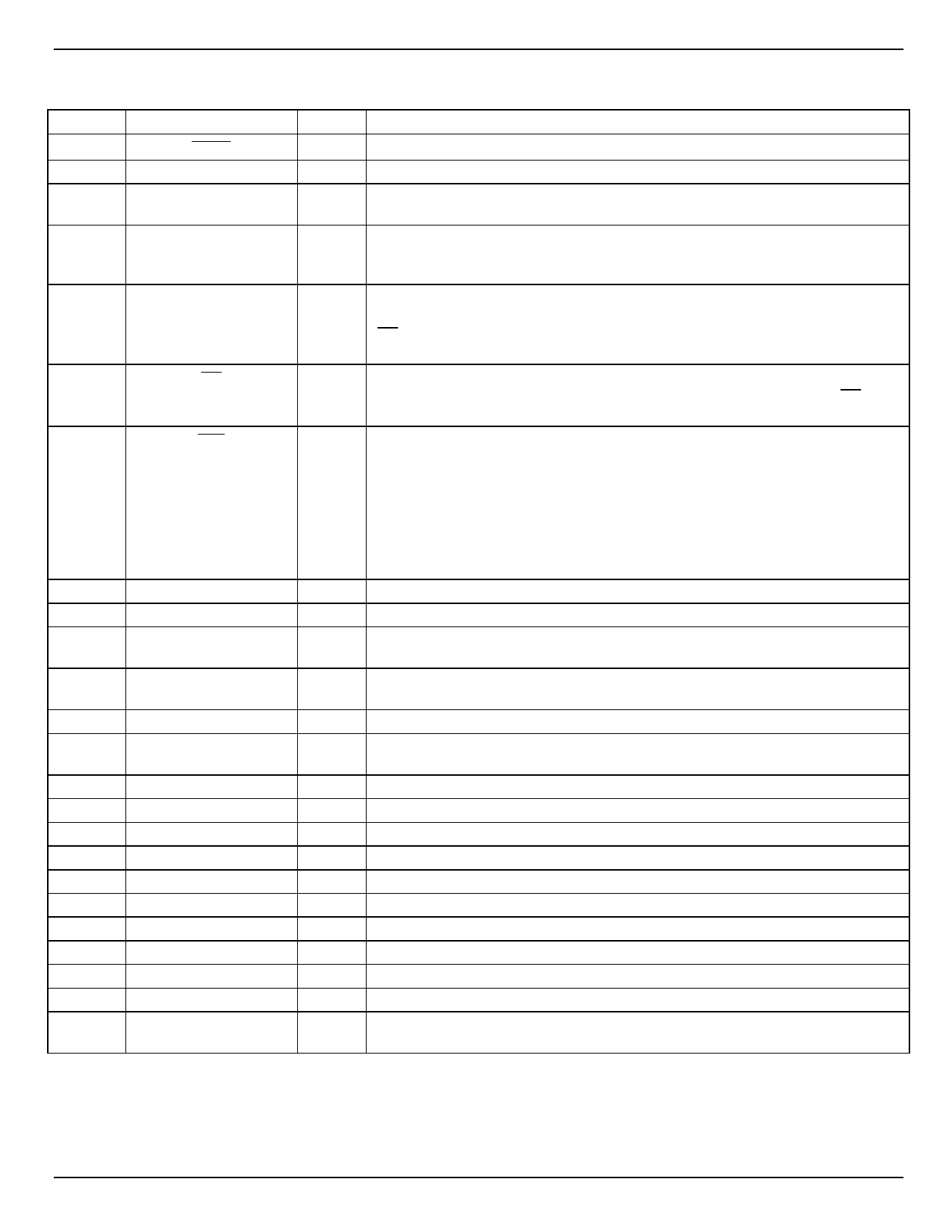
2. Signal List
Pin No.
1
2
3
4
5
6
7
8
9
10
11
12
13
14
15
16
17
18
19
20
21
22
23
24
Name
XTAL
XTAL/CLOCK
SERIAL CLOCK
COMMAND DATA
REPLY DATA
CS
IRQ
COMPOUT
COMPIN
A/D CAP 1
A/D CAP 2
VSS
VBIAS
RX AMP IN
RX AMP OUT
RX AUDIO OUT
TX AUDIO OUT
SUM IN
SUM OUT
MOD1 IN
TX SUB AUDIO OUT
MOD1
MOD2
VDD
Type
output
input
input
input
output
input
output
output
input
output
output
Power
output
input
output
output
output
input
output
input
output
output
output
Power
Description
The inverted output of the on-chip oscillator.
The input to the on-chip oscillator, for external Xtal circuit or clock.
The “C-BUS” serial clock input. This clock, produced by the µC, is used for
timing transfer of commands and data to and from the device. (Figure 4).
The “C-BUS” serial data input from the µC. Data is loaded into this device
in 8-bit bytes, MSB (B7) first, and LSB (B0) last, synchronized to the
SERIAL CLOCK. (Figure 4).
The “C-BUS” serial data output to the µC. The transmission of REPLY
DATA bytes is synchronized to the SERIAL CLOCK under the control of the
CS input. This 3-state output is held at high impedance when not sending
data to the µC. (Figure 4).
The “C-BUS” data loading control function: this input is provided by the µC.
Data transfer sequences are initiated, completed or aborted by the CS
signal (Figure 4).
This output indicates an interrupt condition to the µC by going to a logic "0".
This is a "wire-ORable" output, enabling the connection of up to 8
peripherals to 1 interrupt port on the µC. This pin has a low impedance
pulldown to logic "0" when active and a high-impedance when inactive. An
external pullup resistor is required.
The conditions that cause interrupts are indicated in the IRQ FLAG register
and are effective if not masked out by a corresponding bit in the IRQ MASK
register.
The output of the comparator.
The input to the comparator.
An internal reference voltage for the CTCSS A/D. Bypassed to VSS with an
external capacitor.
An internal reference voltage for the DCS A/D. Bypassed to VSS with an
external capacitor.
Negative supply (ground).
A bias line for the internal circuitry, held at VDD/2. This pin must be
bypassed by a capacitor mounted close to the device pins.
The inverting input to the Rx input amplifier.
Output of the Rx input amplifier
Output of the Rx audio filter section.
Output of the SelCall tone generator.
Input to the audio summing amplifier.
Output of the audio summing amplifier.
Input to MOD1 audio gain control.
Output of the CTCSS or DCS Tx tone generator.
Output of MOD1 audio gain control.
Output of MOD2 audio gain control.
Positive supply. Levels and voltages are dependent upon this supply. This
pin should be bypassed to VSS by a capacitor.
Table 1: Signal List
© 1997 MX•COM Inc.
www.mxcom.com Tele: 800 638-5577 336 744-5050 Fax: 336 744-5054
Doc. # 20480161.002
4800 Bethania Station Road, Winston-Salem, NC 27105-1201 USA
All trademarks and service marks are held by their respective companies.
Share Link: 