TDA16846 Ver la hoja de datos (PDF) - Infineon Technologies
Número de pieza
componentes Descripción
Fabricante
TDA16846
Infineon Technologies

TDA16846 Datasheet PDF : 28 Pages
| |||
TDA 16846
TDA 16846-2
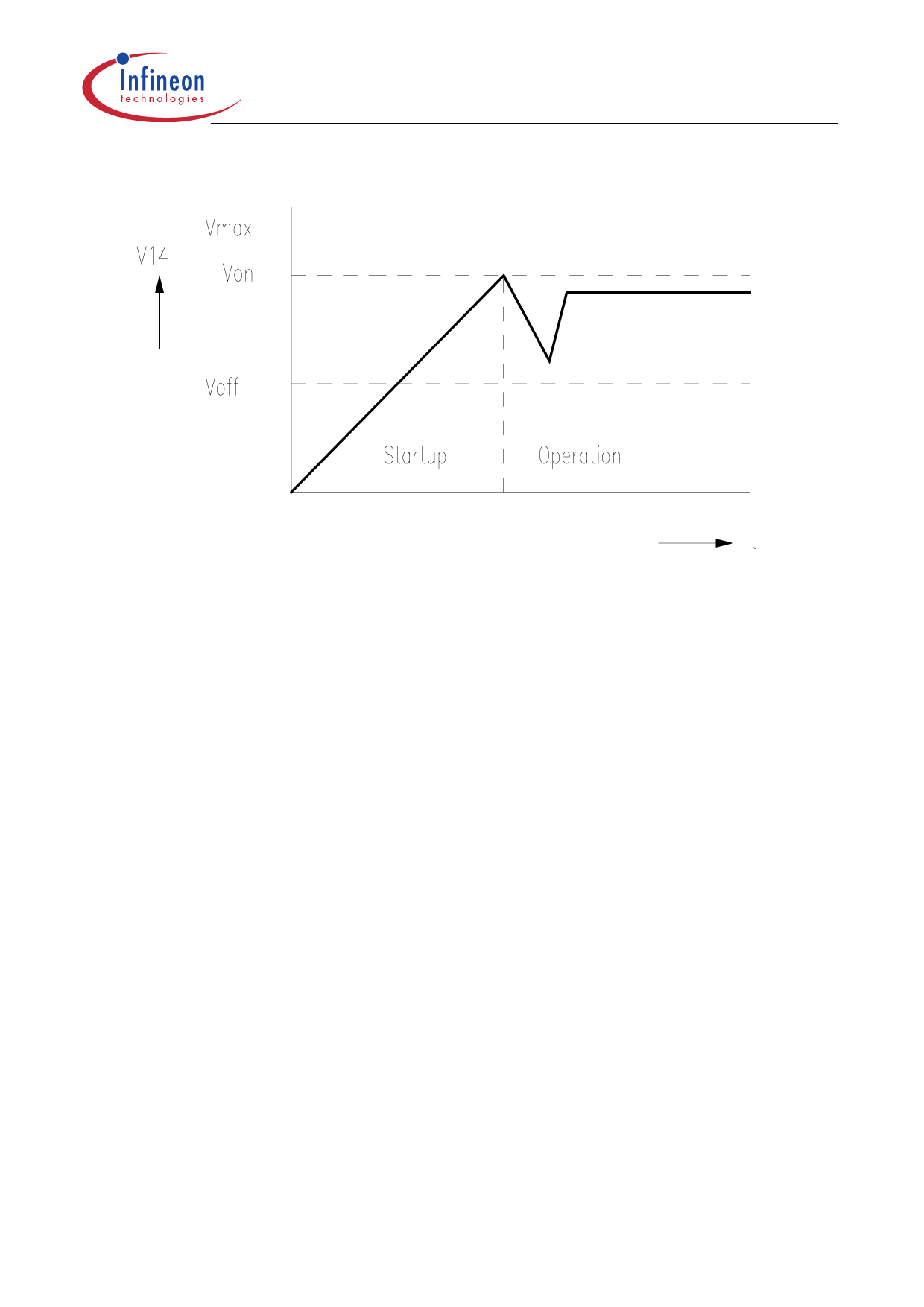
Figure 5 Startup Voltage Diagram
Primary Current Simulation PCS (Pin 2) / Current Limiting
A voltage proportional to the current of the power transistor is generated at Pin 2 by the
RC-combination R2, C2 (Figure 4). The voltage at Pin 2 is forced to 1.5 V when the
power transistor is switched off and during its switch on time C2 is charged by R2 from
the rectified mains. The equation of V2 and the current in the power transistor (Iprimary) is
:
V2
=
1,5 V +
L---p--r--i-m--a--r-y---×----I-p--r--i-m--a--r-y
R2 × C2
Lprimary: Primary inductance of the transformer
The voltage V2 is applied to one input of the On Time Comparator ONTC (see Figure 2).
The other input is the control voltage. If V2 exceeds the control voltage, the driver
switches off (current limiting). The maximum value of the control voltage is the internal
reference voltage 5 V, so the maximum current in the power transistor (IMprimary) is
:
IMprimary
= 3--,--5-----V------×-----R----2----×----C-----2-
Lprimary
The control voltage can be reduced by either the Error Amplifier EA (current mode
regulation), or by an opto coupler at Pin 5 (regulation with opto coupler isolation) or by
the voltage V11 at Pin 11 (Fold Back Point Correction).
Data Sheet
9
2003-07-31
Share Link: