SAA1310T Ver la hoja de datos (PDF) - Philips Electronics
Número de pieza
componentes Descripción
Fabricante
SAA1310T Datasheet PDF : 15 Pages
| |||
Philips Semiconductors
Control interface for VHS video recorders
Product specification
SAA1310
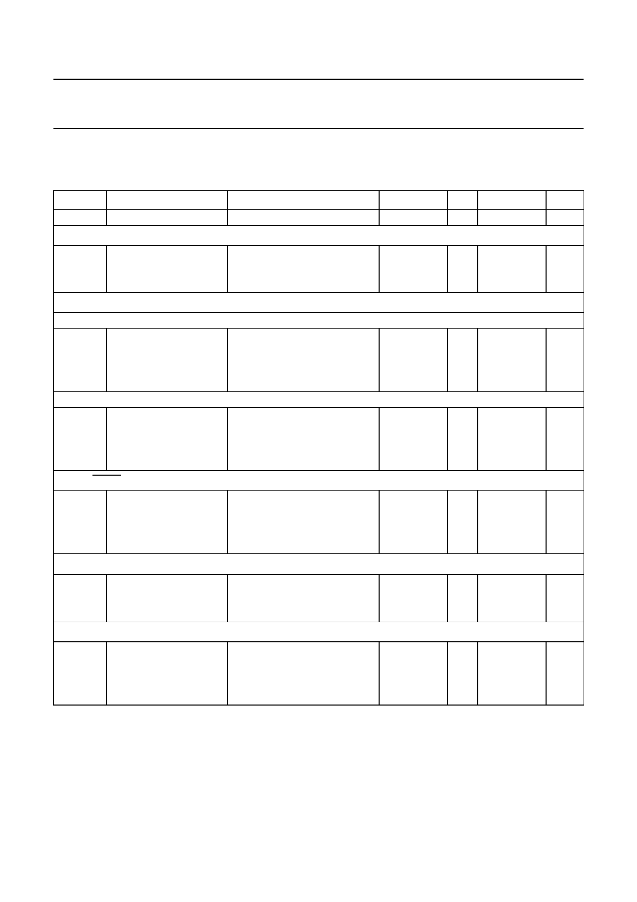
CHARACTERISTICS (PIN NUMBERS IN PARENTHESIS REFER TO SAA1310T)
VP = 5 V; Tamb = 25 °C; all voltage referenced to pin 12 (13); according to the test set-up (see Fig.4); unless otherwise
specified
SYMBOL
PARAMETER
Pd
power dissipation
Supply pin 9 (10)
VP
supply voltage
IP
supply current
CONDITION
note 1
MIN.
−
TYP.
MAX.
85 −
UNIT
mW
4.5
5.0 5.5
V
read mode
10
15 20
mA
write mode; duty factor = 50% 13
18 24
mA
CTL I/O pin 2 (2)
READ MODE PIN 10 (11) < 0.5 V
VI
input voltage (peak-to- f = 500 Hz
0.35
−−
mV
peak value)
f = 30 kHz; non-linear operation −
− 200
mV
B
bandwidth low-pass filter
−
3−
kHz
Ib
input bias current
WRITE MODE PIN 10 (11) > 3.5 V
read mode
−
0.1 −
µA
VO
output voltage LOW
ICTL I/O = 3 mA;
−
pin CTL DATA = HIGH
− 0.4
V
VO
output voltage HIGH
ICTL I/O = − 3 mA;
4.6
−−
V
pin CTL DATA = LOW
WRITE/READ pin 10 (11)
VI
input voltage
II
input current
read mode
write mode; analog
read mode
write mode
−
− 0.5
V
1.6
− 3.3
V
−
− 1.5 −
µA
−
0.1 −
µA
Vref pin 3 (3); note 2
VO
output voltage
2.4
2.5 2.6
V
Itot
total current
including write current
−4
− +4
mA
RO
output resistance
−
0.4 0.6
Ω
CAPREV pin 18 (20)
VIH
input voltage HIGH
VIL
input voltage LOW
IIH
input current HIGH
VCAPREV = 5 V
IIH
input current LOW
VCAPREV = 0 V
2.0
−−
V
−
− 0.8
V
−
− 10
µA
−10
−−
µA
April 1995
6
Share Link: 