TZA3023 Ver la hoja de datos (PDF) - Philips Electronics
Número de pieza
componentes Descripción
Fabricante
TZA3023 Datasheet PDF : 24 Pages
| |||
Philips Semiconductors
SDH/SONET STM4/OC12
transimpedance amplifier
Product specification
TZA3023
PIN diode bias voltage DREF
The transimpedance amplifier together with the PIN diode
determines the performance of an optical receiver for a
large extent. Especially how the PIN diode is connected to
the input and the layout around the input pin influence the
key parameters like sensitivity, bandwidth and the Power
Supply Rejection Ratio (PSRR) of a transimpedance
amplifier. The total capacitance at the input pin is critical to
obtain the highest sensitivity. It should be kept to a
minimum by reducing the capacitor of the PIN diode and
the parasitics around the input pin. The PIN diode should
be placed very close to the IC to reduce the parasitics.
Because the capacitance of the PIN diode depends on the
reverse voltage across it, the reverse voltage should be
chosen as high as possible.
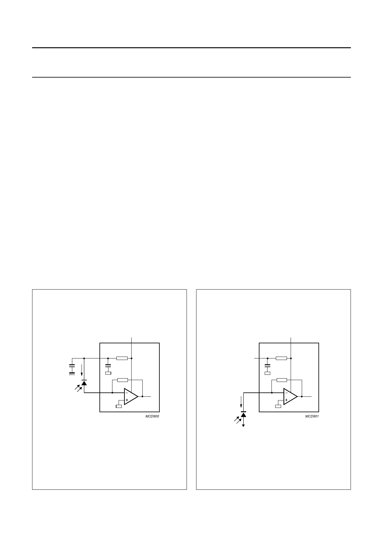
The PIN diode can be connected to the input in two ways
as shown in Figs 5 and 6. In Fig.5 the PIN diode is
connected between DREF and IPhoto. Pin DREF provides
an easy bias voltage for the PIN diode. The voltage at
DREF is derived from VCC by a low-pass filter. The
low-pass filter consisting of the internal resistor R1, C1 and
the external capacitor C2 rejects the supply voltage noise.
The external capacitor C2 should be equal or larger then
1 nF for a high PSRR.
The reverse voltage across the PIN diode is 4.2 V
(5 − 0.8 V) for 5 V supply or 2.5 V (3.3 − 0.8 V) for 3.3 V
supply.
The DC voltage at DREF decreases with increasing signal
levels. Consequently the reverse voltage across the
PIN diode will also decrease with increasing signal levels.
This can be explained with an example. When the
PIN diode delivers a peak-to-peak current of 1 mA, the
average DC current will be 0.5 mA. This DC current is
delivered by VCC through the internal resistor R1 of 2 kΩ
which will cause a voltage drop of 1 V across the resistor
and the reverse voltage across the PIN diode will be
reduced by 1 V.
It is preferable to connect the cathode of the PIN diode to
a higher voltage then VCC when such a voltage source is
available on the board. In this case pin DREF can be left
unconnected. When a negative supply voltage is available,
the configuration in Fig.6 can be used. It should be noted
that in this case the direction of the signal current is
reversed compared to Fig.5. Proper filtering of the bias
voltage for the PIN diode is essential to achieve the
highest sensitivity level.
C2
1 nF
VCC
DREF
4
Ii
R1 8
2 kΩ
C1
10 pF
7
IPhoto
TZA3023
MCD900
VCC
DREF
4
R1 8
2 kΩ
C1
10 pF
IPhoto 7
Ii
negative supply voltage
TZA3023
MCD901
Fig.5 The PIN diode connected between the input
and pin DREF.
Fig.6 The PIN diode connected between the input
and a negative supply voltage.
2000 Mar 29
5
Share Link: 