K305(2004) Ver la hoja de datos (PDF) - STMicroelectronics
Número de pieza
componentes Descripción
Fabricante
K305 Datasheet PDF : 21 Pages
| |||
TSH350
Electrical Characteristics
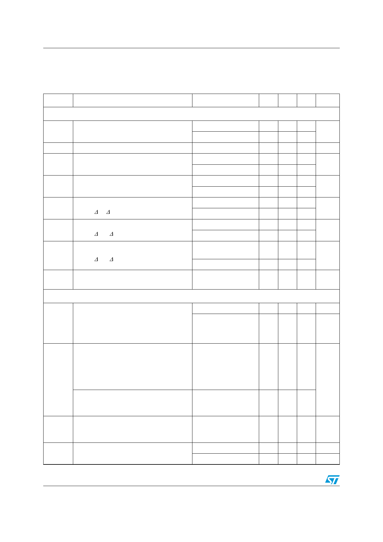
Table 3: Electrical characteristics for VCC = ±2.5Volts, Tamb = 25°C (unless otherwise specified)
Symbol
Parameter
Test Condition
Iout
Isink
Short-circuit Output current coming in
the op-amp.
See fig-8 for more details
Isource
Output current coming out from the op-
amp.
See fig-11 for more details
Noise and distortion
eN
Equivalent Input Noise Voltage
see application note on page 13
Equivalent Input Noise Current (+)
see application note on page 13
iN
Equivalent Input Noise Current (-)
see application note on page 13
SFDR
Spurious Free Dynamic Range
The highest harmonic of the output
spectrum when injecting a filtered sine
wave
Output to GND
Tmin. < Tamb < Tmax.
Output to GND
Tmin. < Tamb < Tmax.
F = 100kHz
F = 100kHz
F = 100kHz
AV = +1, Vout = 1Vp-p
F = 10MHz
F = 20MHz
F = 50MHz
F = 100MHz
Min.
135
-140
Typ.
205
195
-210
-185
Max.
Unit
mA
1.5
nV/√Hz
20
pA/√Hz
13
pA/√Hz
-66
-57
dBc
-46
-42
Table 4: Closed-loop gain and feedback components
VCC (V)
±2.5
Gain
+10
-10
+2
-2
+1
-1
Rfb (Ω)
300
300
300
300
820
300
-3dB Bw (MHz)
125
120
390
370
550
350
0.1dB Bw (MHz)
22
20
110
70
65
120
4/21
Share Link: 