TSC102 Ver la hoja de datos (PDF) - STMicroelectronics
Número de pieza
componentes Descripción
Fabricante
TSC102 Datasheet PDF : 23 Pages
| |||
TSC102
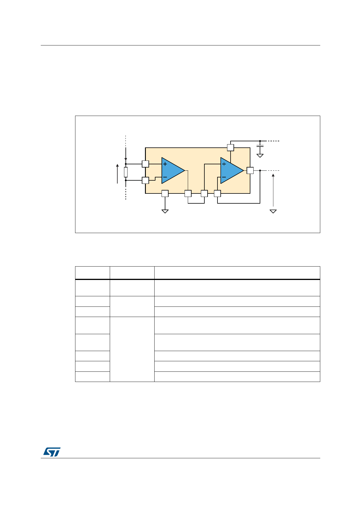
Application schematic and pin description
1
Application schematic and pin description
The TSC102 high-side current sense amplifier features a 2.8 V to 30 V input common-mode
range that is independent of the supply voltage. The main advantage of this feature is that it
allows high-side current sensing at voltages much greater than the supply voltage (VCC).
Figure 1. Application schematics
Current
sense
amplifier
Signal
conditioning
amplifier
5V
Iload Vp
TSC102
6
Vcc
8
Out
Rsense Vm
Av=20 V/V
5
1
Vsense
Gnd
2
A1
A2
3
4
A3
7
Vout
AM04508
Table 1 describes the function of each pin. Their position is shown in the illustration on the
cover page and in Figure 1 above.
Symbol
Out
Gnd
VCC
Vp
Vm
A1
A2
A3
Table 1. Pin description
Type
Function
Analog output
Power supply
Analog input
Out voltage is proportional to the magnitude of the sense voltage
Vp-Vm
Ground line
Positive power supply line
Connection for the external sense resistor. The measured current
enters the shunt on the Vp side
Connection for the external sense resistor. The measured current
exits the shunt on the Vm side
Connection to current sensing amplifier output
Connection to signal conditioning amplifier non-inverting input
Connection to signal conditioning amplifier inverting input
DocID16754 Rev 3
3/23
23
Share Link: 