TQ1090-MC Ver la hoja de datos (PDF) - TriQuint Semiconductor
Número de pieza
componentes Descripción
Fabricante
TQ1090-MC Datasheet PDF : 10 Pages
| |||

TQ1090
Table 2. Phase Shift Selection
S0
S1
Phase Shift (Group A: Q0 – Q4)
0
0
+t
1
0
0
0
1
–t
1
1
–2t
Table 2. Test Mode Selection
Test
Mode
Ref. Clock
1
÷2
fREF
Group A
Outputs Q0–Q4
fREF ÷ 8
Group B
Outputs Q5–Q18
fREF ÷ 4
Group C
Outputs Q9–Q10
fREF ÷ 2
Layout Guidelines
Multiple ground and power pins on the TQ1090 reduce
ground bounce. Good layout techniques, however, are
necessary to guarantee proper operation and to meet
the specifications across the full operating range. We
recommend bypassing each of the VDD supply pins to
the nearest ground pin, as close to the chip as possible.
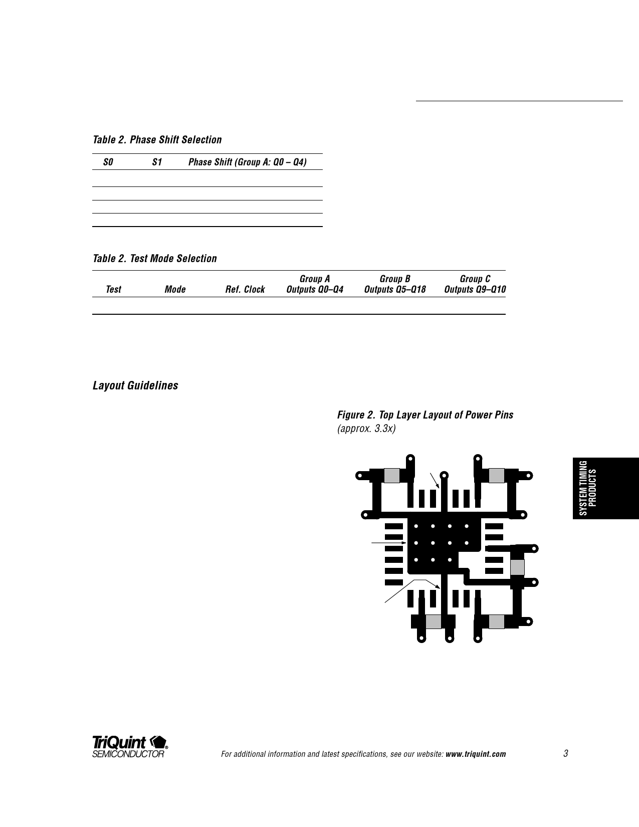
Figure 2. Top Layer Layout of Power Pins
(approx. 3.3x)
VDD
VDD
C4
C3
Pin 1
Figure 2 shows the recommended power layout for the
TQ1090. The bypass capacitors should be located on
the same side of the board as the TQ1090. The VDD
traces connect to an inner-layer VDD plane. All of the
ground pins (GND) are connected to a small ground
plane on the surface beneath the chip. Multiple
through-holes connect this small surface plane to an
inner-layer ground plane. The capacitors (C1–C5) are
0.1 mF. TriQuint’s test board uses X7R temperature-
stable capacitors in 1206 SMD cases.
Ground
Plane
Pin 15
C5
VDD
VDD
C2
C1
VDD
For additional information and latest specifications, see our website: www.triquint.com
3